32-Bit
Microcontroller
TC212 / TC213 / TC214 / TC222 /
TC223 / TC224
32-Bit Single-Chip Micocontroller
AC-Step
32-Bit Single-Chip Micocontroller
Data Sheet
V 1.0, 2017-09
Microcontrollers
�Edition 2017-09
Published by
Infineon Technologies AG
81726 Munich, Germany
© 2017 Infineon Technologies AG
All Rights Reserved.
Legal Disclaimer
The information given in this document shall in no event be regarded as a guarantee of conditions or
characteristics. With respect to any examples or hints given herein, any typical values stated herein and/or any
information regarding the application of the device, Infineon Technologies hereby disclaims any and all warranties
and liabilities of any kind, including without limitation, warranties of non-infringement of intellectual property rights
of any third party.
Information
For further information on technology, delivery terms and conditions and prices, please contact the nearest
Infineon Technologies Office (www.infineon.com)
Warnings
Due to technical requirements, components may contain dangerous substances. For information on the types in
question, please contact the nearest Infineon Technologies Office.
Infineon Technologies components may be used in life-support devices or systems only with the express written
approval of Infineon Technologies, if a failure of such components can reasonably be expected to cause the failure
of that life-support device or system or to affect the safety or effectiveness of that device or system. Life support
devices or systems are intended to be implanted in the human body or to support and/or maintain and sustain
and/or protect human life. If they fail, it is reasonable to assume that the health of the user or other persons may
be endangered.
�TC212 / TC213 / TC214 / TC222 / TC223 / TC224
Revision History
Page or Item
Subjects (major changes since previous revision)
V 1.0, 2017-09
The history is documented in the last chapter
Data Sheet
3
V 1.0 2017-09
�TC212 / TC213 / TC214 / TC222 / TC223 / TC224
Trademarks of Infineon Technologies AG
AURIX™, C166™, CanPAK™, CIPOS™, CIPURSE™, EconoPACK™, CoolMOS™, CoolSET™,
CORECONTROL™, CROSSAVE™, DAVE™, DI-POL™, EasyPIM™, EconoBRIDGE™, EconoDUAL™,
EconoPIM™, EconoPACK™, EiceDRIVER™, eupec™, FCOS™, HITFET™, HybridPACK™, I²RF™,
ISOFACE™, IsoPACK™, MIPAQ™, ModSTACK™, my-d™, NovalithIC™, OptiMOS™, ORIGA™,
POWERCODE™; PRIMARION™, PrimePACK™, PrimeSTACK™, PRO-SIL™, PROFET™, RASIC™,
ReverSave™, SatRIC™, SIEGET™, SINDRION™, SIPMOS™, SmartLEWIS™, SOLID FLASH™, TEMPFET™,
thinQ!™, TRENCHSTOP™, TriCore™.
Other Trademarks
Advance Design System™ (ADS) of Agilent Technologies, AMBA™, ARM™, MULTI-ICE™, KEIL™,
PRIMECELL™, REALVIEW™, THUMB™, µVision™ of ARM Limited, UK. AUTOSAR™ is licensed by AUTOSAR
development partnership. Bluetooth™ of Bluetooth SIG Inc. CAT-iq™ of DECT Forum. COLOSSUS™,
FirstGPS™ of Trimble Navigation Ltd. EMV™ of EMVCo, LLC (Visa Holdings Inc.). EPCOS™ of Epcos AG.
FLEXGO™ of Microsoft Corporation. FlexRay™ is licensed by FlexRay Consortium. HYPERTERMINAL™ of
Hilgraeve Incorporated. IEC™ of Commission Electrotechnique Internationale. IrDA™ of Infrared Data
Association Corporation. ISO™ of INTERNATIONAL ORGANIZATION FOR STANDARDIZATION. MATLAB™ of
MathWorks, Inc. MAXIM™ of Maxim Integrated Products, Inc. MICROTEC™, NUCLEUS™ of Mentor Graphics
Corporation. MIPI™ of MIPI Alliance, Inc. MIPS™ of MIPS Technologies, Inc., USA. muRata™ of MURATA
MANUFACTURING CO., MICROWAVE OFFICE™ (MWO) of Applied Wave Research Inc., OmniVision™ of
OmniVision Technologies, Inc. Openwave™ Openwave Systems Inc. RED HAT™ Red Hat, Inc. RFMD™ RF
Micro Devices, Inc. SIRIUS™ of Sirius Satellite Radio Inc. SOLARIS™ of Sun Microsystems, Inc. SPANSION™
of Spansion LLC Ltd. Symbian™ of Symbian Software Limited. TAIYO YUDEN™ of Taiyo Yuden Co.
TEAKLITE™ of CEVA, Inc. TEKTRONIX™ of Tektronix Inc. TOKO™ of TOKO KABUSHIKI KAISHA TA. UNIX™
of X/Open Company Limited. VERILOG™, PALLADIUM™ of Cadence Design Systems, Inc. VLYNQ™ of Texas
Instruments Incorporated. VXWORKS™, WIND RIVER™ of WIND RIVER SYSTEMS, INC. ZETEX™ of Diodes
Zetex Limited.
Last Trademarks Update 2011-11-11
Data Sheet
4
V 1.0 2017-09
�TC212 / TC213 / TC214 / TC222 / TC223 / TC224
Table of Contents
1
Summary of Features . . . . . . . . . . . . . . . . . . . . . . . . . . . . . . . . . . . . . . . . . . . . . . . . . . . . . . . . . . . . . 1
2
2.1
2.1.1
2.1.1.1
2.1.1.2
2.1.2
2.2
2.2.1
2.2.1.1
2.2.1.2
2.2.2
2.3
2.3.1
2.3.1.1
2.3.1.2
2.3.2
Package and Pinning Definitions . . . . . . . . . . . . . . . . . . . . . . . . . . . . . . . . . . . . . . . . . . . . . . . . . . . 5
PG-TQFP-80-7 Package Variant Pin Configuration of TC212 / TC222 . . . . . . . . . . . . . . . . . . . . . . . . 5
Port Functions and Pinning Tables . . . . . . . . . . . . . . . . . . . . . . . . . . . . . . . . . . . . . . . . . . . . . . . . . . 6
How to Read the Following Port Function Tables . . . . . . . . . . . . . . . . . . . . . . . . . . . . . . . . . . . . . 6
Tables . . . . . . . . . . . . . . . . . . . . . . . . . . . . . . . . . . . . . . . . . . . . . . . . . . . . . . . . . . . . . . . . . . . . . . 7
Pull-Up/Pull-Down Reset Behavior of the Pins . . . . . . . . . . . . . . . . . . . . . . . . . . . . . . . . . . . . . . . . 38
PG-TQFP-100-23 Package Variant Pin Configuration of TC213 / TC223 . . . . . . . . . . . . . . . . . . . . . 38
Port Functions and Pinning Tables . . . . . . . . . . . . . . . . . . . . . . . . . . . . . . . . . . . . . . . . . . . . . . . . . 40
How to Read the Following Port Function Tables . . . . . . . . . . . . . . . . . . . . . . . . . . . . . . . . . . . . 40
Tables . . . . . . . . . . . . . . . . . . . . . . . . . . . . . . . . . . . . . . . . . . . . . . . . . . . . . . . . . . . . . . . . . . . . . 41
Pull-Up/Pull-Down Reset Behavior of the Pins . . . . . . . . . . . . . . . . . . . . . . . . . . . . . . . . . . . . . . . . 77
PG-TQFP-144-27 Package Variant Pin Configuration of TC214 / TC224 . . . . . . . . . . . . . . . . . . . . . 77
Port Functions and Pinning Tables . . . . . . . . . . . . . . . . . . . . . . . . . . . . . . . . . . . . . . . . . . . . . . . . . 79
How to Read the Following Port Function Tables . . . . . . . . . . . . . . . . . . . . . . . . . . . . . . . . . . . . 79
Tables . . . . . . . . . . . . . . . . . . . . . . . . . . . . . . . . . . . . . . . . . . . . . . . . . . . . . . . . . . . . . . . . . . . . . 80
Pull-Up/Pull-Down Reset Behavior of the Pins . . . . . . . . . . . . . . . . . . . . . . . . . . . . . . . . . . . . . . . 136
3
3.1
3.2
3.3
3.4
3.5
3.6
3.7
3.8
3.9
3.10
3.10.1
3.11
3.11.1
3.11.2
3.12
3.13
3.14
3.15
3.16
3.17
3.18
3.19
3.20
3.21
3.21.1
3.22
Electrical Specification . . . . . . . . . . . . . . . . . . . . . . . . . . . . . . . . . . . . . . . . . . . . . . . . . . . . . . . . .
Parameter Interpretation . . . . . . . . . . . . . . . . . . . . . . . . . . . . . . . . . . . . . . . . . . . . . . . . . . . . . . . . . .
Absolute Maximum Ratings . . . . . . . . . . . . . . . . . . . . . . . . . . . . . . . . . . . . . . . . . . . . . . . . . . . . . . .
Pin Reliability in Overload . . . . . . . . . . . . . . . . . . . . . . . . . . . . . . . . . . . . . . . . . . . . . . . . . . . . . . . . .
Operating Conditions . . . . . . . . . . . . . . . . . . . . . . . . . . . . . . . . . . . . . . . . . . . . . . . . . . . . . . . . . . . .
3.3 V Pads . . . . . . . . . . . . . . . . . . . . . . . . . . . . . . . . . . . . . . . . . . . . . . . . . . . . . . . . . . . . . . . . . . . .
VADC Parameters . . . . . . . . . . . . . . . . . . . . . . . . . . . . . . . . . . . . . . . . . . . . . . . . . . . . . . . . . . . . . .
MHz Oscillator . . . . . . . . . . . . . . . . . . . . . . . . . . . . . . . . . . . . . . . . . . . . . . . . . . . . . . . . . . . . . . . . .
Back-up Clock . . . . . . . . . . . . . . . . . . . . . . . . . . . . . . . . . . . . . . . . . . . . . . . . . . . . . . . . . . . . . . . . . .
Temperature Sensor . . . . . . . . . . . . . . . . . . . . . . . . . . . . . . . . . . . . . . . . . . . . . . . . . . . . . . . . . . . . .
Power Supply Current . . . . . . . . . . . . . . . . . . . . . . . . . . . . . . . . . . . . . . . . . . . . . . . . . . . . . . . . . . . .
Calculating the 1.3 V Current Consumption . . . . . . . . . . . . . . . . . . . . . . . . . . . . . . . . . . . . . . . . .
Power-up and Power-down . . . . . . . . . . . . . . . . . . . . . . . . . . . . . . . . . . . . . . . . . . . . . . . . . . . . . . .
Single Supply mode . . . . . . . . . . . . . . . . . . . . . . . . . . . . . . . . . . . . . . . . . . . . . . . . . . . . . . . . . . .
External Supply mode . . . . . . . . . . . . . . . . . . . . . . . . . . . . . . . . . . . . . . . . . . . . . . . . . . . . . . . . . .
Reset Timing . . . . . . . . . . . . . . . . . . . . . . . . . . . . . . . . . . . . . . . . . . . . . . . . . . . . . . . . . . . . . . . . . . .
EVR . . . . . . . . . . . . . . . . . . . . . . . . . . . . . . . . . . . . . . . . . . . . . . . . . . . . . . . . . . . . . . . . . . . . . . . . .
Phase Locked Loop (PLL) . . . . . . . . . . . . . . . . . . . . . . . . . . . . . . . . . . . . . . . . . . . . . . . . . . . . . . . .
AC Specifications . . . . . . . . . . . . . . . . . . . . . . . . . . . . . . . . . . . . . . . . . . . . . . . . . . . . . . . . . . . . . . .
JTAG Parameters . . . . . . . . . . . . . . . . . . . . . . . . . . . . . . . . . . . . . . . . . . . . . . . . . . . . . . . . . . . . . . .
DAP Parameters . . . . . . . . . . . . . . . . . . . . . . . . . . . . . . . . . . . . . . . . . . . . . . . . . . . . . . . . . . . . . . . .
ASCLIN SPI Master Timing . . . . . . . . . . . . . . . . . . . . . . . . . . . . . . . . . . . . . . . . . . . . . . . . . . . . . . .
QSPI Timings, Master and Slave Mode . . . . . . . . . . . . . . . . . . . . . . . . . . . . . . . . . . . . . . . . . . . . . .
Flash Parameters . . . . . . . . . . . . . . . . . . . . . . . . . . . . . . . . . . . . . . . . . . . . . . . . . . . . . . . . . . . . . . .
Package Outline . . . . . . . . . . . . . . . . . . . . . . . . . . . . . . . . . . . . . . . . . . . . . . . . . . . . . . . . . . . . . . . .
Package Parameters . . . . . . . . . . . . . . . . . . . . . . . . . . . . . . . . . . . . . . . . . . . . . . . . . . . . . . . . . . .
Quality Declarations . . . . . . . . . . . . . . . . . . . . . . . . . . . . . . . . . . . . . . . . . . . . . . . . . . . . . . . . . . . . .
4
4.1
History . . . . . . . . . . . . . . . . . . . . . . . . . . . . . . . . . . . . . . . . . . . . . . . . . . . . . . . . . . . . . . . . . . . . . . . 185
Changes from Version TC21x22x_DS_V1.0 to Version TC21x22x_AC_DS_V1.0 . . . . . . . . . . . . . 185
Data Sheet
TOC-1
137
137
138
139
141
143
147
152
153
154
155
156
157
158
160
161
163
165
166
167
169
171
173
177
180
182
184
V 1.0, 2017-09
�TC212 / TC213 / TC214 / TC222 / TC223 / TC224
Summary of Features
1
Summary of Features
The TC22x / TC21x product family has the following features:
•
High Performance Microcontroller with one CPU core
•
Power Efficient scalar TriCore CPU (TC1.6E), having the following features:
–
Binary code compatibility with TC1.6P
–
133 MHz operation at full temperature range
–
88 Kbyte Data Scratch-Pad RAM (DSPR)
–
8 Kbyte Instruction Scratch-Pad RAM (PSPR)
–
8 Kbyte Instruction Cache (ICACHE)
–
4 line read buffer (DRB)
•
Lockstepped shadow core for TC1.6E
•
Multiple on-chip memories
–
All embedded NVM and SRAM are ECC protected
–
1 Mbyte Program Flash Memory (PFLASH)
–
96 Kbyte Data Flash Memory (DFLASH) usable for EEPROM emulation
–
BootROM (BROM)
•
16-Channel DMA Controller with safe data transfer
•
Sophisticated interrupt system (ECC protected)
•
High performance on-chip bus structure
–
64-bit Cross Bar Interconnect (SRI) giving fast parallel access between bus masters, CPUs and memories
–
32-bit System Peripheral Bus (SPB) for on-chip peripheral and functional units
–
One bus bridge (SFI Bridge)
•
Safety Management Unit (SMU) handling safety monitor alarms
•
Memory Test Unit with ECC, Memory Initialization and MBIST functions (MTU)
•
Hardware I/O Monitor (IOM) for checking of digital I/O
•
Versatile On-chip Peripheral Units
•
–
Two Asynchronous/Synchronous Serial Channels (ASCLIN) with hardware LIN support (V1.3, V2.0, V2.1
and J2602) up to 50 MBaud
–
Four Queued SPI Interface Channels (QSPI) with master and slave capability up to 50 Mbit/s
–
One MultiCAN+ Module with 3 CAN nodes each and 128 free assignable message objects for high
efficiency data handling via FIFO buffering and gateway data transfer
–
4 Single Edge Nibble Transmission (SENT) channels for connection to sensors
–
One Generic Timer Module (GTM) providing a powerful set of digital signal filtering and timer functionality
to realize autonomous and complex Input/Output management
–
One Capture / Compare 6 module (Two kernels CCU60 and CCU61)
–
One General Purpose 12 Timer Unit (GPT120)
Versatile Successive Approximation ADC (VADC)
–
Cluster of 2 independent ADC kernels
–
Input voltage range from 0 V to 5.5V (ADC supply)
•
Digital programmable I/O ports
•
On-chip debug support for OCDS Level 1 (CPUs, DMA, On Chip Buses)
•
Four/five wire JTAG (IEEE 1149.1) or DAP (Device Access Port) interface
Data Sheet
1-1
V 1.0 2017-09
�TC212 / TC213 / TC214 / TC222 / TC223 / TC224
Summary of Features
•
Power Management System and on-chip regulators
•
Clock Generation Unit with System PLL
•
Embedded Voltage Regulator
Data Sheet
1-2
V 1.0 2017-09
�TC212 / TC213 / TC214 / TC222 / TC223 / TC224
Summary of Features
Ordering Information
The ordering code for Infineon microcontrollers provides an exact reference to the required product. This ordering
code identifies:
•
The derivative itself, i.e. its function set, the temperature range, and the supply voltage
•
The package and the type of delivery.
For the available ordering codes for the TC212 / TC213 / TC214 / TC222 / TC223 / TC224 please refer to the
“AURIX™ TC2x Data Sheet Addendum”, which summarizes all available variants.
Table 1-1
Overview of TC21x / TC22x Functions
Feature
CPU Core
TC1.6E
Type
E Cores / Checker Cores
1/
1
133 MHz
Max. Freq.
FPU
yes
Program Flash
Size
1 Mbyte
Data Flash
Size
96 Kbyte
Cache
Instruction
8 Kbyte
4 line read buffer
Data
88 Kbyte / 8 Kbyte 1)
SRAM
Size TC1.6E
(DSPR/PSPR)
DMA
Channels
16
ADC
Channels
12+12
Converter
2
TIM
1
TOM
2
DTM
2
GTM
1/1
CMU / ICM
1
TBU
Timer
1
GPT12
1
CCU6
STM
Modules
1
CAN
Modules
1
Nodes per Module
3
Message Objects
128
yes
CAN FD
QSPI
Channels
4
ASCLIN
Interfaces
2
SENT
Channels
4
ASIL
Level
Data Sheet
up to ASIL-D
1-3
V 1.0 2017-09
�TC212 / TC213 / TC214 / TC222 / TC223 / TC224
Summary of Features
Table 1-1
Overview of TC21x / TC22x Functions
Feature
Safety support
1
SMU
1
IOM
0
FFT
2
HSIC
Channels
Embedded Voltage Regulator
LDO from 3.3 V to 1.3 V
Yes
Low Power Feature
Standby RAM
Yes
Packages
Type
PG-TQFP-80-7 / PG-TQFP-10023 / PG-TQFP-144-27
I/O
Type
3.3 V CMOS (5V input supported on
ADC pins)
Tambient
Range
−40 … +125°C / +150°C
1) To ensure the processor cores are provided with a constant stream of instructions the Instruction Fetch Units will
speculatively fetch instructions from the up to 64 bytes ahead of the current PC.
If the current PC is within 64 bytes of the top of an instruction memory the Instruction Fetch Unit may attempt to
speculatively fetch instruction from beyond the physical range. This may then lead to error conditions and alarms being
triggered by the bus and memory systems.
It is therefore recommended that the upper 64 bytes of any memory be unused for instruction storage.
Data Sheet
1-4
V 1.0 2017-09
�TC212 / TC213 / TC214 / TC222 / TC223 / TC224
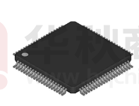
Package and Pinning DefinitionsPG-TQFP-80-7 Package Variant Pin
2
Package and Pinning Definitions
This chapter gives a pinning of the different packages of the TC212 / TC213 / TC214 / TC222 / TC223 / TC224.
2.1
PG-TQFP-80-7 Package Variant Pin Configuration of TC212 / TC222
80
79
78
77
76
75
74
73
72
71
70
69
68
67
66
65
64
63
62
61
P10.6
P10.5
P11.12
P11.11
P11.10
P11.9
P11.6
P11.3
P11.2
V DDP3
P14.6
P14.4
P14.3
P14.1/B ootloader
P14.0/B ootloader
P15.5
P15.3
P15.2
P15.1
P15.0
Figure 2-1 is showing the TC212 / TC222 pinout for the package variant PG-TQFP-80-7.
1
2
3
4
5
6
7
8
9
10
11
12
13
14
15
16
17
18
19
20
TC22x
(Top View)
60
59
58
57
56
55
54
53
52
51
50
49
48
47
46
45
44
43
42
41
P20.14
P20.13
P20.12
P20.11
P20.9
P20.8
VDD
PORST
ESR1
P20.2/TESTMODE
TCK/ DAP0
TRST
P21.7/TDO/DAP2
TMS/DAP1
P21.6/TDI
VDDP 3
XTAL2
XTAL1
VDD
P23.1
AN10/P 40.10
AN9/P 40.9
AN8/P 40.8
AN7/P 40.7
VAGND
VAR E F
VS SM
VDDM
AN6/P 40.6
AN5/P 40.5
P 33.5
P 33.6
P 33.7
P 33.8
P 33.9
P 33.10
V DDP 3
N.C .
N.C .
N.C .
21
22
23
24
25
26
27
28
29
30
31
32
33
34
35
36
37
38
39
40
P02.0
P02.1
P02.2
P02.3
P02.4
P02.5
P02.6
P02.7
P02.8
P00.0
VDD
V DDP3
AN18/P41.6
AN17/P41.5
AN16/P41.4
AN15/P41.3
AN14/P41.2
AN13/P41.1
AN12/P41.0
AN11/P40.11
Figure 2-1 TC212 / TC222 Pinout for the package variant PG-TQFP-80-7
Data Sheet
2-5
V 1.0 2017-09
�TC212 / TC213 / TC214 / TC222 / TC223 / TC224
Package and Pinning DefinitionsPG-TQFP-80-7 Package Variant Pin
2.1.1
Port Functions and Pinning Tables
2.1.1.1
How to Read the Following Port Function Tables
Some hints for interpreting the following tables.
Column “Ctrl.”:
I = Input (for GPIO port Lines with IOCR bit field Selection PCx = 0XXXB)
AI = Analog input
O = Output
O0 = Output with IOCR bit field selection PCx = 1X000B
O1 = Output with IOCR bit field selection PCx = 1X001B (ALT1)
O2 = Output with IOCR bit field selection PCx = 1X010B (ALT2)
O3 = Output with IOCR bit field selection PCx = 1X011B (ALT3)
O4 = Output with IOCR bit field selection PCx = 1X100B (ALT4)
O5 = Output with IOCR bit field selection PCx = 1X101B (ALT5)
O6 = Output with IOCR bit field selection PCx = 1X110B (ALT6)
O7 = Output with IOCR bit field selection PCx = 1X111B (ALT7)
Table 2-1
Example Port Table
Pin
Symbol
Ctrl.
Buffer
Type
10
Pxx.y
I
A1 / HighZ / General-purpose input
VDDP3
GTM_TIN
TIMm_n
TOMa_b
O1
Function
GTM_TOUT
TOMc_d
GTM_TOUT
IOM_REFv_w
IOM reference input
ASCLINz_RTS
O2
ASCLIN0 output (aka ARTSz)
To each input several functions can be connected. The peripherals’ configuration defines if this input is used.
The port module (see corresponding chapter) decides which of the 8 output signals O0 to O7 drives the pad.
Some Ox rows list more than one function, e.g. several GTM_TOUT outputs and IOM reference inputs. The GTM
module (see corresponding chapter) has its own sub-multiplexer structure that defines which of the GTM sub-units
drives this signal. Additionally the IOM modules “listens” on these output signals (see IOM chapter).
Some pin symbol names were changed in this AURIX device compared to other AURIX devices to improve naming
systematics. The previously used symbol name is documented in the “Function” column with the text “(aka …)”1).
Column “Type”:
IN = Input only
A1 = Pad class A1 (3.3V)
A1+ = Pad class A1+ (3.3V)
S = ADC with digital input. Pad class D for analog input “AI”, pad class S for digital input “I”.
PU = with pull-up device connected during reset (PORST = 0)
PD = with pull-down device connected during reset (PORST = 0)
1) “aka” as abbreviation for “also known as”.
Data Sheet
2-6
V 1.0 2017-09
�TC212 / TC213 / TC214 / TC222 / TC223 / TC224
Package and Pinning DefinitionsPG-TQFP-80-7 Package Variant Pin
High-Z = High-Z during reset (PORST = 0)
Vx = Supply (the Exposed Pad is also considered as VSS and shall be connected to ground)
2.1.1.2
Tables
Port function and pinning tables.
Table 2-2
Port 00 Functions
Pin
Symbol
Ctrl.
Buffer
Type
Function
10
P00.0
I
A1 /
HighZ /
VDDP3
General-purpose input
TIM0_0
CCU61_CTRAPA
CCU60_T12HRE
GTM_TIN
CCU61 input
CCU60 input
P00.0
O0
General-purpose output
TOM0_8
O1
GTM_TOUT
TOM1_0
GTM_TOUT
TOM0_4
GTM_TOUT (= DTM1_OUT4)
TOM1_4
GTM_TOUT (= DTM5_OUT4)
IOM_REF0_9
IOM reference input
ASCLIN0_SCLK
O2
ASCLIN0 output (aka: ASCLK0)
ASCLIN0_TX
O3
ASCLIN0 output (aka: ATX0)
IOM_MON2_12
IOM monitor input
IOM_REF2_12
IOM reference input
—
O4
Reserved
CAN1_TXD
O5
CAN node 1 output (aka: TXDCAN1)
IOM_MON2_6
IOM monitor input
IOM_REF2_6
IOM reference input
—
O6
Reserved
CCU60_COUT63
O7
CCU60 output
IOM_MON1_6
IOM monitor input
IOM_REF1_0
IOM reference input
Data Sheet
2-7
V 1.0 2017-09
�TC212 / TC213 / TC214 / TC222 / TC223 / TC224
Package and Pinning DefinitionsPG-TQFP-80-7 Package Variant Pin
Table 2-3
Port 02 Functions
Pin
Symbol
Ctrl.
Buffer
Type
Function
1
P02.0
I
A1+ /
HighZ /
VDDP3
General-purpose input
TIM0_0
SCU_REQ6
GTM_TIN
SCU input
CCU60_CC60INA
CCU60 input
CCU61_CC60INB
CCU61 input
P02.0
O0
General-purpose output
TOM0_8
O1
GTM_TOUT
TOM1_8
GTM_TOUT
TOM0_4
GTM_TOUT (= DTM1_OUT4)
TOM1_4
GTM_TOUT (= DTM5_OUT4)
IOM_REF0_0
IOM reference input
—
O2
Reserved
QSPI3_SLSO1
O3
QSPI3 output (aka: SLSO31)
—
O4
Reserved
CAN0_TXD
O5
CAN node 0 output (aka: TXDCAN0)
IOM_MON2_5
IOM monitor input
IOM_REF2_5
IOM reference input
—
O6
Reserved
CCU60_CC60
O7
CCU60 output
IOM_MON1_2
IOM monitor input
IOM_REF1_6
IOM reference input
Data Sheet
2-8
V 1.0 2017-09
�TC212 / TC213 / TC214 / TC222 / TC223 / TC224
Package and Pinning DefinitionsPG-TQFP-80-7 Package Variant Pin
Table 2-3
Port 02 Functions (cont’d)
Pin
Symbol
Ctrl.
Buffer
Type
Function
2
P02.1
I
A1 /
HighZ /
VDDP3
General-purpose input
TIM0_1
CAN0_RXDA
SCU_REQ14
GTM_TIN
CAN node 0 input (aka: RXDCAN0A)
SCU input
P02.1
O0
General-purpose output
TOM0_9
O1
GTM_TOUT
TOM1_9
GTM_TOUT
TOM0_4N
GTM_TOUT (= DTM1_OUT4_N)
TOM1_4N
GTM_TOUT (= DTM5_OUT4_N)
IOM_REF0_1
IOM reference input
—
O2
Reserved
QSPI3_SLSO2
O3
QSPI3 output (aka: SLSO32)
—
O4
Reserved
—
O5
Reserved
—
O6
Reserved
CCU60_COUT60
O7
CCU60 output
IOM_MON1_3
IOM monitor input
IOM_REF1_3
IOM reference input
Data Sheet
2-9
V 1.0 2017-09
�TC212 / TC213 / TC214 / TC222 / TC223 / TC224
Package and Pinning DefinitionsPG-TQFP-80-7 Package Variant Pin
Table 2-3
Port 02 Functions (cont’d)
Pin
Symbol
Ctrl.
Buffer
Type
Function
3
P02.2
I
A1+ /
HighZ /
VDDP3
General-purpose input
TIM0_2
CCU60_CC61INA
CCU61_CC61INB
GTM_TIN
CCU60 input
CCU61 input
P02.2
O0
General-purpose output
TOM0_10
O1
GTM_TOUT
TOM1_10
GTM_TOUT
TOM0_5
GTM_TOUT (= DTM1_OUT5)
TOM1_5
GTM_TOUT (= DTM5_OUT5)
IOM_REF0_2
IOM reference input
ASCLIN1_TX
O2
ASCLIN1 output (aka: ATX1)
IOM_MON2_13
IOM monitor input
IOM_REF2_13
IOM reference input
QSPI3_SLSO3
O3
QSPI3 output (aka: SLSO33)
—
O4
Reserved
CAN2_TXD
O5
CAN node 2 output (aka: TXDCAN2)
IOM_MON2_7
IOM monitor input
IOM_REF2_7
IOM reference input
—
O6
Reserved
CCU60_CC61
O7
CCU60 output
IOM_MON1_1
IOM monitor input
IOM_REF1_5
IOM reference input
Data Sheet
2-10
V 1.0 2017-09
�TC212 / TC213 / TC214 / TC222 / TC223 / TC224
Package and Pinning DefinitionsPG-TQFP-80-7 Package Variant Pin
Table 2-3
Port 02 Functions (cont’d)
Pin
Symbol
Ctrl.
Buffer
Type
Function
4
P02.3
I
A1 /
HighZ /
VDDP3
General-purpose input
TIM0_3
ASCLIN1_RXG
CAN2_RXDB
5
GTM_TIN
ASCLIN1 input (aka: ARX1G)
CAN node 2 input (aka: RXDCAN2B)
P02.3
O0
General-purpose output
TOM0_11
O1
GTM_TOUT
TOM1_11
GTM_TOUT
TOM0_5N
GTM_TOUT (= DTM1_OUT5_N)
TOM1_5N
GTM_TOUT (= DTM5_OUT5_N)
IOM_REF0_3
IOM reference input
—
O2
Reserved
QSPI3_SLSO4
O3
QSPI3 output (aka: SLSO34)
—
O4
Reserved
—
O5
Reserved
—
O6
Reserved
CCU60_COUT61
O7
CCU60 output
IOM_MON1_4
IOM monitor input
IOM_REF1_2
IOM reference input
P02.4
I
TIM0_4
QSPI3_SLSIA
A1+ /
HighZ /
VDDP3
General-purpose input
GTM_TIN
QSPI3 input (aka: SLSI3A)
CAN0_RXDD
CAN node 0 input (aka: RXDCAN0D)
CCU60_CC62INA
CCU60 input
CCU61_CC62INB
CCU61 input
P02.4
O0
General-purpose output
TOM0_12
O1
GTM_TOUT
TOM1_12
GTM_TOUT
TOM0_6
GTM_TOUT (= DTM1_OUT6)
TOM1_6
GTM_TOUT (= DTM5_OUT6)
IOM_REF0_4
IOM reference input
—
O2
Reserved
QSPI3_SLSO0
O3
QSPI3 output (aka: SLSO30)
—
O4
Reserved
—
O5
Reserved
—
O6
Reserved
CCU60_CC62
O7
CCU60 output
IOM_MON1_0
IOM monitor input
IOM_REF1_4
IOM reference input
Data Sheet
2-11
V 1.0 2017-09
�TC212 / TC213 / TC214 / TC222 / TC223 / TC224
Package and Pinning DefinitionsPG-TQFP-80-7 Package Variant Pin
Table 2-3
Port 02 Functions (cont’d)
Pin
Symbol
Ctrl.
Buffer
Type
Function
6
P02.5
I
A1+ /
HighZ /
VDDP3
General-purpose input
TIM0_5
QSPI3_MRSTA
SENT_SENT3C
GTM_TIN
QSPI3 input (aka: MRST3A)
SENT input
P02.5
O0
General-purpose output
TOM0_13
O1
GTM_TOUT
TOM1_13
GTM_TOUT
TOM0_6N
GTM_TOUT (= DTM1_OUT6_N)
TOM1_6N
GTM_TOUT (= DTM5_OUT6_N)
IOM_REF0_5
IOM reference input
CAN0_TXD
O2
CAN node 0 output (aka: TXDCAN0)
IOM_MON2_5
IOM monitor input
IOM_REF2_5
IOM reference input
QSPI3_MRST
O3
QSPI3 output (aka: MRST3)
IOM_MON2_3
IOM monitor input
IOM_REF2_3
IOM reference input
—
O4
Reserved
—
O5
Reserved
—
O6
Reserved
CCU60_COUT62
O7
CCU60 output
IOM_MON1_5
IOM monitor input
IOM_REF1_1
IOM reference input
Data Sheet
2-12
V 1.0 2017-09
�TC212 / TC213 / TC214 / TC222 / TC223 / TC224
Package and Pinning DefinitionsPG-TQFP-80-7 Package Variant Pin
Table 2-3
Port 02 Functions (cont’d)
Pin
Symbol
Ctrl.
Buffer
Type
Function
7
P02.6
I
A1 /
HighZ /
VDDP3
General-purpose input
TIM0_6
QSPI3_MTSRA
GTM_TIN
QSPI3 input (aka: MTSR3A)
SENT_SENT2C
SENT input
CCU60_CC60INC
CCU60 input
CCU60_CCPOS0A
CCU60 input
CCU61_T12HRB
CCU61 input
GPT120_T3INA
GPT120 input
P02.6
O0
General-purpose output
TOM0_14
O1
GTM_TOUT
TOM1_14
GTM_TOUT
TOM0_7
GTM_TOUT (= DTM1_OUT7)
TOM1_7
GTM_TOUT (= DTM5_OUT7)
IOM_REF0_6
IOM reference input
—
O2
Reserved
QSPI3_MTSR
O3
QSPI3 output (aka: MTSR3)
—
O4
Reserved
VADC_EMUX00
O5
VADC output
—
O6
Reserved
CCU60_CC60
O7
CCU60 output
IOM_MON1_2
IOM monitor input
IOM_REF1_6
IOM reference input
Data Sheet
2-13
V 1.0 2017-09
�TC212 / TC213 / TC214 / TC222 / TC223 / TC224
Package and Pinning DefinitionsPG-TQFP-80-7 Package Variant Pin
Table 2-3
Port 02 Functions (cont’d)
Pin
Symbol
Ctrl.
Buffer
Type
Function
8
P02.7
I
A1 /
HighZ /
VDDP3
General-purpose input
TIM0_7
QSPI3_SCLKA
GTM_TIN
QSPI3 input (aka: SCLK3A)
SENT_SENT1C
SENT input
CCU60_CC61INC
CCU60 input
CCU60_CCPOS1A
CCU60 input
CCU61_T13HRB
CCU61 input
GPT120_T3EUDA
GPT120 input
PMU_FDEST
PMU input
P02.7
O0
General-purpose output
TOM0_15
O1
GTM_TOUT
TOM1_15
GTM_TOUT
TOM0_7N
GTM_TOUT (= DTM1_OUT7_N)
TOM1_7N
GTM_TOUT (= DTM5_OUT7_N)
IOM_REF0_7
IOM reference input
—
O2
Reserved
QSPI3_SCLK
O3
QSPI3 output (aka: SCLK3)
—
O4
Reserved
VADC_EMUX01
O5
VADC output
SENT_SPC1
O6
SENT output
CCU60_CC61
O7
CCU60 output
IOM_MON1_1
IOM monitor input
IOM_REF1_5
IOM reference input
Data Sheet
2-14
V 1.0 2017-09
�TC212 / TC213 / TC214 / TC222 / TC223 / TC224
Package and Pinning DefinitionsPG-TQFP-80-7 Package Variant Pin
Table 2-3
Port 02 Functions (cont’d)
Pin
Symbol
Ctrl.
Buffer
Type
Function
9
P02.8
I
A1 /
HighZ /
VDDP3
General-purpose input
TIM0_0
SENT_SENT0C
GTM_TIN
SENT input
CCU60_CC62INC
CCU60 input
CCU60_CCPOS2A
CCU60 input
CCU61_T12HRC
CCU61 input
CCU61_T13HRC
CCU61 input
GPT120_T4INA
GPT120 input
P02.8
O0
General-purpose output
TOM0_8
O1
GTM_TOUT
TOM1_0
GTM_TOUT
TOM0_4N
GTM_TOUT (= DTM1_OUT4_N)
TOM1_4N
GTM_TOUT (= DTM5_OUT4_N)
IOM_REF0_8
IOM reference input
QSPI3_SLSO5
O2
QSPI3 output (aka: SLSO35)
—
O3
Reserved
—
O4
Reserved
VADC_EMUX02
O5
VADC output
—
O6
Reserved
CCU60_CC62
O7
CCU60 output
IOM_MON1_0
IOM monitor input
IOM_REF1_4
IOM reference input
Data Sheet
2-15
V 1.0 2017-09
�TC212 / TC213 / TC214 / TC222 / TC223 / TC224
Package and Pinning DefinitionsPG-TQFP-80-7 Package Variant Pin
Table 2-4
Port 10 Functions
Pin
Symbol
Ctrl.
Buffer
Type
Function
79
P10.5
I
A1 /
HighZ /
VDDP3
General-purpose input
TIM0_2
SCU_HWCFG4
80
GTM_TIN
SCU input
P10.5
O0
General-purpose output
TOM0_2
O1
GTM_TOUT
TOM1_10
GTM_TOUT
IOM_REF2_9
IOM reference input
—
O2
Reserved
QSPI3_SLSO8
O3
QSPI3 output (aka: SLSO38)
QSPI1_SLSO9
O4
QSPI1 output (aka: SLSO19)
GPT120_T6OUT
O5
GPT120 output
—
O6
Reserved
—
O7
Reserved
P10.6
I
TIM0_3
QSPI3_MTSRB
SCU_HWCFG5
A1 /
HighZ /
VDDP3
General-purpose input
GTM_TIN
QSPI3 input (aka: MTSR3B)
SCU input
P10.6
O0
General-purpose output
TOM0_3
O1
GTM_TOUT
TOM1_11
GTM_TOUT
IOM_REF2_10
IOM reference input
—
O2
Reserved
QSPI3_MTSR
O3
QSPI3 output (aka: MTSR3)
GPT120_T3OUT
O4
GPT120 output
—
O5
Reserved
QSPI1_MRST
O6
QSPI1 output (aka: MRST1)
IOM_MON2_1
IOM monitor input
IOM_REF2_1
IOM reference input
—
Data Sheet
O7
Reserved
2-16
V 1.0 2017-09
�TC212 / TC213 / TC214 / TC222 / TC223 / TC224
Package and Pinning DefinitionsPG-TQFP-80-7 Package Variant Pin
Table 2-5
Port 11 Functions
Pin
Symbol
Ctrl.
Buffer
Type
Function
72
P11.2
I
General-purpose input
P11.2
O0
TOM0_8
O1
A1+ /
HighZ /
VDDP3
73
General-purpose output
GTM_TOUT
TOM1_1
GTM_TOUT
TOM0_4N
GTM_TOUT (= DTM1_OUT4_N)
TOM1_4N
GTM_TOUT (= DTM5_OUT4_N)
—
O2
Reserved
QSPI0_SLSO5
O3
QSPI0 output (aka: SLSO05)
QSPI1_SLSO5
O4
QSPI1 output (aka: SLSO15)
CCU61_COUT63
O5
CCU61 output
IOM_MON1_7
IOM monitor input
IOM_REF1_7
IOM reference input
—
O6
Reserved
CCU60_COUT63
O7
CCU60 output
IOM_MON1_6
IOM monitor input
IOM_REF1_0
IOM reference input
P11.3
I
QSPI1_MRSTB
P11.3
O0
TOM0_10
O1
A1+ /
HighZ /
VDDP3
General-purpose input
QSPI1 input (aka: MRST1B)
General-purpose output
GTM_TOUT
TOM1_2
GTM_TOUT
TOM0_5
GTM_TOUT (= DTM1_OUT5)
TOM1_5
GTM_TOUT (= DTM5_OUT5)
—
O2
Reserved
QSPI1_MRST
O3
QSPI1 output (aka: MRST1)
IOM_MON2_1
IOM monitor input
IOM_REF2_1
IOM reference input
—
O4
Reserved
CCU61_COUT62
O5
CCU61 output
IOM_MON1_13
IOM monitor input
IOM_REF1_8
IOM reference input
—
O6
Reserved
CCU60_COUT62
O7
CCU60 output
IOM_MON1_5
IOM monitor input
IOM_REF1_1
IOM reference input
Data Sheet
2-17
V 1.0 2017-09
�TC212 / TC213 / TC214 / TC222 / TC223 / TC224
Package and Pinning DefinitionsPG-TQFP-80-7 Package Variant Pin
Table 2-5
Port 11 Functions (cont’d)
Pin
Symbol
Ctrl.
Buffer
Type
Function
74
P11.6
I
A1+ /
HighZ /
VDDP3
General-purpose input
QSPI1_SCLKB
75
P11.6
O0
TOM0_11
O1
QSPI1 input (aka: SCLK1B)
General-purpose output
GTM_TOUT
TOM1_3
GTM_TOUT
TOM0_5N
GTM_TOUT (= DTM1_OUT5_N)
TOM1_5N
GTM_TOUT (= DTM5_OUT5_N)
—
O2
Reserved
QSPI1_SCLK
O3
QSPI1 output (aka: SCLK1)
—
O4
Reserved
CCU61_COUT61
O5
CCU61 output
IOM_MON1_12
IOM monitor input
IOM_REF1_9
IOM reference input
—
O6
Reserved
CCU60_COUT61
O7
CCU60 output
IOM_MON1_4
IOM monitor input
IOM_REF1_2
IOM reference input
P11.9
I
QSPI1_MTSRB
P11.9
O0
TOM0_12
O1
A1+ /
HighZ /
VDDP3
General-purpose input
QSPI1 input (aka: MTSR1B)
General-purpose output
GTM_TOUT
TOM1_4
GTM_TOUT (= DTM5_OUT4)
TOM0_6
GTM_TOUT (= DTM1_OUT6)
TOM1_6
GTM_TOUT (= DTM5_OUT6)
—
O2
Reserved
QSPI1_MTSR
O3
QSPI1 output (aka: MTSR1)
—
O4
Reserved
CCU61_COUT60
O5
CCU61 output
IOM_MON1_11
IOM monitor input
IOM_REF1_10
IOM reference input
—
O6
Reserved
CCU60_COUT60
O7
CCU60 output
IOM_MON1_3
IOM monitor input
IOM_REF1_3
IOM reference input
Data Sheet
2-18
V 1.0 2017-09
�TC212 / TC213 / TC214 / TC222 / TC223 / TC224
Package and Pinning DefinitionsPG-TQFP-80-7 Package Variant Pin
Table 2-5
Port 11 Functions (cont’d)
Pin
Symbol
Ctrl.
Buffer
Type
Function
76
P11.10
I
A1+ /
HighZ /
VDDP3
General-purpose input
ASCLIN1_RXE
SCU_REQ12
77
ASCLIN1 input (aka: ARX1E)
SCU input
P11.10
O0
General-purpose output
TOM0_13
O1
GTM_TOUT
TOM1_5
GTM_TOUT (= DTM5_OUT5)
TOM0_6N
GTM_TOUT (= DTM1_OUT6_N)
TOM1_6N
GTM_TOUT (= DTM5_OUT6_N)
—
O2
Reserved
QSPI0_SLSO3
O3
QSPI0 output (aka: SLSO03)
QSPI1_SLSO3
O4
QSPI1 output (aka: SLSO13)
CCU61_CC62
O5
CCU61 output
IOM_MON1_10
IOM monitor input
IOM_REF1_11
IOM reference input
—
O6
Reserved
CCU60_CC62
O7
CCU60 output
IOM_MON1_0
IOM monitor input
IOM_REF1_4
IOM reference input
P11.11
I
P11.11
O0
TOM0_14
O1
A1+ /
HighZ /
VDDP3
General-purpose input
General-purpose output
GTM_TOUT
TOM1_6
GTM_TOUT (= DTM5_OUT6)
TOM0_7N
GTM_TOUT (= DTM1_OUT7_N)
TOM1_7N
GTM_TOUT (= DTM5_OUT7_N)
—
O2
Reserved
QSPI0_SLSO4
O3
QSPI0 output (aka: SLSO04)
QSPI1_SLSO4
O4
QSPI1 output (aka: SLSO14)
CCU61_CC61
O5
CCU61 output
IOM_MON1_9
IOM monitor input
IOM_REF1_12
IOM reference input
—
O6
Reserved
CCU60_CC61
O7
CCU60 output
IOM_MON1_1
IOM monitor input
IOM_REF1_5
IOM reference input
Data Sheet
2-19
V 1.0 2017-09
�TC212 / TC213 / TC214 / TC222 / TC223 / TC224
Package and Pinning DefinitionsPG-TQFP-80-7 Package Variant Pin
Table 2-5
Port 11 Functions (cont’d)
Pin
Symbol
Ctrl.
Buffer
Type
Function
78
P11.12
I
General-purpose input
P11.12
O0
TOM0_15
O1
A1+ /
HighZ /
VDDP3
General-purpose output
GTM_TOUT
TOM1_7
GTM_TOUT (= DTM5_OUT7)
TOM0_7
GTM_TOUT (= DTM1_OUT7)
TOM1_7
GTM_TOUT (= DTM5_OUT7)
ASCLIN1_TX
O2
ASCLIN1 output (aka: ATX1)
IOM_MON2_13
IOM monitor input
IOM_REF2_13
IOM reference input
GTM_CLK2
O3
GTM output
—
O4
Reserved
CCU61_CC60
O5
CCU61 output
IOM_MON1_8
IOM monitor input
IOM_REF1_13
IOM reference input
SCU_EXTCLK1
O6
SCU output
CCU60_CC60
O7
CCU60 output
IOM_MON1_2
IOM monitor input
IOM_REF1_6
IOM reference input
Data Sheet
2-20
V 1.0 2017-09
�TC212 / TC213 / TC214 / TC222 / TC223 / TC224
Package and Pinning DefinitionsPG-TQFP-80-7 Package Variant Pin
Table 2-6
Port 14 Functions
Pin
Symbol
Ctrl.
Buffer
Type
Function
66
P14.0
I
A1+ /
HighZ /
VDDP3
General-purpose input
TIM0_3
P14.0
O0
TOM0_3
O1
GTM_TIN
General-purpose output
GTM_TOUT
TOM1_3
GTM_TOUT
TOM0_6
GTM_TOUT (= DTM1_OUT6)
TOM1_6
GTM_TOUT (= DTM5_OUT6)
ASCLIN0_TX
O2
ASCLIN0 output (aka: ATX0)
IOM_MON2_12
IOM monitor input
IOM_REF2_12
IOM reference input
—
O3
Reserved
—
O4
Reserved
CAN1_TXD
O5
CAN node 1 output (aka: TXDCAN1)
IOM_MON2_6
IOM monitor input
IOM_REF2_6
IOM reference input
ASCLIN0_SCLK
O6
ASCLIN0 output (aka: ASCLK0)
CCU60_COUT62
O7
CCU60 output
IOM_MON1_5
IOM monitor input
IOM_REF1_1
IOM reference input
Data Sheet
2-21
V 1.0 2017-09
�TC212 / TC213 / TC214 / TC222 / TC223 / TC224
Package and Pinning DefinitionsPG-TQFP-80-7 Package Variant Pin
Table 2-6
Port 14 Functions (cont’d)
Pin
Symbol
Ctrl.
Buffer
Type
Function
67
P14.1
I
A1+ /
HighZ /
VDDP3
General-purpose input
TIM0_4
ASCLIN0_RXA
ASCLIN0 input (aka: ARX0A)
CAN1_RXDB
CAN node 1 input (aka: RXDCAN1B)
SCU_REQ15
SCU input
SCU_EVRWUPA
AI
SCU input
P14.1
O0
General-purpose output
TOM0_4
O1
GTM_TOUT (= DTM1_OUT4)
TOM1_4
GTM_TOUT (= DTM5_OUT4)
TOM0_7
GTM_TOUT (= DTM1_OUT7)
TOM1_7
GTM_TOUT (= DTM5_OUT7)
IOM_REF1_14
IOM reference input
ASCLIN0_TX
68
GTM_TIN
O2
ASCLIN0 output (aka: ATX0)
IOM_MON2_12
IOM monitor input
IOM_REF2_12
IOM reference input
—
O3
Reserved
—
O4
Reserved
—
O5
Reserved
—
O6
Reserved
CCU60_COUT63
O7
CCU60 output
IOM_MON1_6
IOM monitor input
IOM_REF1_0
IOM reference input
P14.3
I
TIM0_6
A1 / PU /
VDDP3
General-purpose input
GTM_TIN
SCU_REQ10
SCU input
SCU_HWCFG3_BMI
SCU input
P14.3
O0
General-purpose output
TOM0_6
O1
GTM_TOUT (= DTM1_OUT6)
TOM1_6
GTM_TOUT (= DTM5_OUT6)
IOM_REF2_4
IOM reference input
—
O2
Reserved
QSPI2_SLSO3
O3
QSPI2 output (aka: SLSO23)
ASCLIN1_SLSO
O4
ASCLIN1 output (aka: ASLSO1)
—
O5
Reserved
—
O6
Reserved
—
O7
Reserved
Data Sheet
2-22
V 1.0 2017-09
�TC212 / TC213 / TC214 / TC222 / TC223 / TC224
Package and Pinning DefinitionsPG-TQFP-80-7 Package Variant Pin
Table 2-6
Port 14 Functions (cont’d)
Pin
Symbol
Ctrl.
Buffer
Type
Function
69
P14.4
I
A1+ /
HighZ /
VDDP3
General-purpose input
TIM0_7
70
P14.4
O0
TOM0_7
O1
GTM_TIN
General-purpose output
GTM_TOUT (= DTM1_OUT7)
TOM1_7
GTM_TOUT (= DTM5_OUT7)
TOM0_7N
GTM_TOUT (= DTM1_OUT7_N)
TOM1_7N
GTM_TOUT (= DTM5_OUT7_N)
IOM_REF2_8
IOM reference input
—
O2
Reserved
—
O3
Reserved
—
O4
Reserved
—
O5
Reserved
—
O6
Reserved
—
O7
Reserved
P14.6
I
TIM0_1
QSPI0_MRSTD
A1+ / PU / General-purpose input
VDDP3
GTM_TIN
QSPI0 input (aka: MRST0D)
P14.6
O0
General-purpose output
TOM0_1
O1
GTM_TOUT
TOM1_1
GTM_TOUT
IOM_REF2_14
IOM reference input
—
O2
Reserved
QSPI2_SLSO2
O3
QSPI2 output (aka: SLSO22)
—
O4
Reserved
—
O5
Reserved
—
O6
Reserved
—
O7
Reserved
Data Sheet
2-23
V 1.0 2017-09
�TC212 / TC213 / TC214 / TC222 / TC223 / TC224
Package and Pinning DefinitionsPG-TQFP-80-7 Package Variant Pin
Table 2-7
Port 15 Functions
Pin
Symbol
Ctrl.
Buffer
Type
Function
61
P15.0
I
General-purpose input
P15.0
O0
TOM1_3
O1
A1 /
HighZ /
VDDP3
GTM_TOUT
TOM0_11
GTM_TOUT
TOM0_7N
GTM_TOUT (= DTM1_OUT7_N)
TOM1_7N
GTM_TOUT (= DTM5_OUT7_N)
ASCLIN1_TX
62
General-purpose output
O2
ASCLIN1 output (aka: ATX1)
IOM_MON2_13
IOM monitor input
IOM_REF2_13
IOM reference input
QSPI0_SLSO13
O3
QSPI0 output (aka: SLSO013)
—
O4
Reserved
CAN2_TXD
O5
CAN node 2 output (aka: TXDCAN2)
IOM_MON2_7
IOM monitor input
IOM_REF2_7
IOM reference input
ASCLIN1_SCLK
O6
ASCLIN1 output (aka: ASCLK1)
—
O7
Reserved
P15.1
I
ASCLIN1_RXA
QSPI2_SLSIB
A1 /
HighZ /
VDDP3
General-purpose input
ASCLIN1 input (aka: ARX1A)
QSPI2 input (aka: SLSI2B)
CAN2_RXDA
CAN node 2 input (aka: RXDCAN2A)
SCU_REQ16
SCU input
SCU_EVRWUPB
AI
SCU input
P15.1
O0
General-purpose output
TOM1_4
O1
GTM_TOUT (= DTM5_OUT4)
TOM0_12
GTM_TOUT
TOM0_4
GTM_TOUT (= DTM1_OUT4)
TOM1_4
GTM_TOUT (= DTM5_OUT4)
ASCLIN1_TX
O2
ASCLIN1 output (aka: ATX1)
IOM_MON2_13
IOM monitor input
IOM_REF2_13
IOM reference input
QSPI2_SLSO5
O3
QSPI2 output (aka: SLSO25)
—
O4
Reserved
—
O5
Reserved
—
O6
Reserved
—
O7
Reserved
Data Sheet
2-24
V 1.0 2017-09
�TC212 / TC213 / TC214 / TC222 / TC223 / TC224
Package and Pinning DefinitionsPG-TQFP-80-7 Package Variant Pin
Table 2-7
Port 15 Functions (cont’d)
Pin
Symbol
Ctrl.
Buffer
Type
Function
63
P15.2
I
A1 /
HighZ /
VDDP3
General-purpose input
QSPI2_MRSTE
QSPI2_SLSIA
QSPI2_HSICINA
QSPI2 input (aka: SLSI2A)
QSPI2 input (aka: HSIC2INA)
P15.2
O0
General-purpose output
TOM1_5
O1
GTM_TOUT (= DTM5_OUT5)
TOM0_13
GTM_TOUT
TOM0_4N
GTM_TOUT (= DTM1_OUT4_N)
TOM1_4N
GTM_TOUT (= DTM5_OUT4_N)
ASCLIN0_TX
64
QSPI2 input (aka: MRST2E)
O2
ASCLIN0 output (aka: ATX0)
IOM_MON2_12
IOM monitor input
IOM_REF2_12
IOM reference input
QSPI2_SLSO0
O3
QSPI2 output (aka: SLSO20)
—
O4
Reserved
CAN1_TXD
O5
CAN node 1 output (aka: TXDCAN1)
IOM_MON2_6
IOM monitor input
IOM_REF2_6
IOM reference input
ASCLIN0_SCLK
O6
ASCLIN0 output (aka: ASCLK0)
—
O7
Reserved
P15.3
I
ASCLIN0_RXB
QSPI2_SCLKA
A1 /
HighZ /
VDDP3
General-purpose input
ASCLIN0 input (aka: ARX0B)
QSPI2 input (aka: SCLK2A)
QSPI2_HSICINB
QSPI2 input (aka: HSIC2INB)
CAN1_RXDA
CAN node 1 input (aka: RXDCAN1A)
P15.3
O0
General-purpose output
TOM1_6
O1
GTM_TOUT (= DTM5_OUT6)
TOM0_14
GTM_TOUT
TOM0_5
GTM_TOUT (= DTM1_OUT5)
TOM1_5
GTM_TOUT (= DTM5_OUT5)
ASCLIN0_TX
O2
ASCLIN0 output (aka: ATX0)
IOM_MON2_12
IOM monitor input
IOM_REF2_12
IOM reference input
QSPI2_SCLK
O3
QSPI2 output (aka: SCLK2)
—
O4
Reserved
—
O5
Reserved
—
O6
Reserved
—
O7
Reserved
Data Sheet
2-25
V 1.0 2017-09
�TC212 / TC213 / TC214 / TC222 / TC223 / TC224
Package and Pinning DefinitionsPG-TQFP-80-7 Package Variant Pin
Table 2-7
Port 15 Functions (cont’d)
Pin
Symbol
Ctrl.
Buffer
Type
Function
65
P15.5
I
A1 /
HighZ /
VDDP3
General-purpose input
ASCLIN1_RXB
QSPI2_MTSRA
SCU_REQ13
ASCLIN1 input (aka: ARX1B)
QSPI2 input (aka: MTSR2A)
SCU input
P15.5
O0
General-purpose output
TOM0_0
O1
GTM_TOUT
TOM1_0
GTM_TOUT
TOM0_5N
GTM_TOUT (= DTM1_OUT5_N)
TOM1_5N
GTM_TOUT (= DTM5_OUT5_N)
ASCLIN1_TX
O2
ASCLIN1 output (aka: ATX1)
IOM_MON2_13
IOM monitor input
IOM_REF2_13
IOM reference input
QSPI2_MTSR
O3
QSPI2 output (aka: MTSR2)
—
O4
Reserved
—
O5
Reserved
—
O6
Reserved
CCU60_CC61
O7
CCU60 output
IOM_MON1_1
IOM monitor input
IOM_REF1_5
IOM reference input
Table 2-8
Port 20 Functions
Pin
Symbol
Ctrl.
Buffer
Type
51
P20.2
I
Input Only General-purpose input
/ PU /
Factory Test Mode Enable
VDDP3
TESTMODE
Data Sheet
Function
2-26
V 1.0 2017-09
�TC212 / TC213 / TC214 / TC222 / TC223 / TC224
Package and Pinning DefinitionsPG-TQFP-80-7 Package Variant Pin
Table 2-8
Port 20 Functions (cont’d)
Pin
Symbol
Ctrl.
Buffer
Type
Function
55
P20.8
I
A1 /
HighZ /
VDDP3
General-purpose input
TIM0_7
56
P20.8
O0
TOM1_7
O1
GTM_TIN
General-purpose output
GTM_TOUT (= DTM5_OUT7)
TOM0_7
GTM_TOUT (= DTM1_OUT7)
TOM0_4
GTM_TOUT (= DTM1_OUT4)
TOM1_4
GTM_TOUT (= DTM5_OUT4)
IOM_MON2_8
IOM monitor input
ASCLIN1_SLSO
O2
ASCLIN1 output (aka: ASLSO1)
QSPI0_SLSO0
O3
QSPI0 output (aka: SLSO00)
QSPI1_SLSO0
O4
QSPI1 output (aka: SLSO10)
CAN0_TXD
O5
CAN node 0 output (aka: TXDCAN0)
IOM_MON2_5
IOM monitor input
IOM_REF2_5
IOM reference input
SCU_WDT0LCK
O6
SCU output
CCU61_CC60
O7
CCU61 output
IOM_MON1_8
IOM monitor input
IOM_REF1_13
IOM reference input
P20.9
I
ASCLIN1_RXC
QSPI0_SLSIB
SCU_REQ11
A1 /
HighZ /
VDDP3
General-purpose input
ASCLIN1 input (aka: ARX1C)
QSPI0 input (aka: SLSI0B)
SCU input
P20.9
O0
General-purpose output
TOM1_13
O1
GTM_TOUT
TOM0_13
GTM_TOUT
TOM0_4N
GTM_TOUT (= DTM1_OUT4_N)
TOM1_4N
GTM_TOUT (= DTM5_OUT4_N)
IOM_MON2_11
IOM monitor input
—
O2
Reserved
QSPI0_SLSO1
O3
QSPI0 output (aka: SLSO01)
QSPI1_SLSO1
O4
QSPI1 output (aka: SLSO11)
—
O5
Reserved
SCU_WDTSLCK
O6
SCU output
CCU61_CC61
O7
CCU61 output
IOM_MON1_9
IOM monitor input
IOM_REF1_12
IOM reference input
Data Sheet
2-27
V 1.0 2017-09
�TC212 / TC213 / TC214 / TC222 / TC223 / TC224
Package and Pinning DefinitionsPG-TQFP-80-7 Package Variant Pin
Table 2-8
Port 20 Functions (cont’d)
Pin
Symbol
Ctrl.
Buffer
Type
Function
57
P20.11
I
A1+ /
HighZ /
VDDP3
General-purpose input
QSPI0_SCLKA
58
P20.11
O0
TOM1_15
O1
QSPI0 input (aka: SCLK0A)
General-purpose output
GTM_TOUT
TOM0_15
GTM_TOUT
TOM0_5N
GTM_TOUT (= DTM1_OUT5_N)
TOM1_5N
GTM_TOUT (= DTM5_OUT5_N)
IOM_MON2_15
IOM monitor input
—
O2
Reserved
QSPI0_SCLK
O3
QSPI0 output (aka: SCLK0)
—
O4
Reserved
—
O5
Reserved
—
O6
Reserved
CCU61_COUT60
O7
CCU61 output
IOM_MON1_11
IOM monitor input
IOM_REF1_10
IOM reference input
P20.12
I
QSPI0_MRSTA
IOM_PIN13
A1 /
HighZ /
VDDP3
General-purpose input
QSPI0 input (aka: MRST0A)
IOM pad input
P20.12
O0
General-purpose output
TOM1_0
O1
GTM_TOUT
TOM0_8
GTM_TOUT
TOM0_6
GTM_TOUT (= DTM1_OUT6)
TOM1_6
GTM_TOUT (= DTM5_OUT6)
IOM_MON0_13
IOM monitor input
—
O2
Reserved
QSPI0_MRST
O3
QSPI0 output (aka: MRST0)
IOM_MON2_0
IOM monitor input
IOM_REF2_0
IOM reference input
QSPI0_MTSR
O4
QSPI0 output (aka: MTSR0)
—
O5
Reserved
—
O6
Reserved
CCU61_COUT61
O7
CCU61 output
IOM_MON1_12
IOM monitor input
IOM_REF1_9
IOM reference input
Data Sheet
2-28
V 1.0 2017-09
�TC212 / TC213 / TC214 / TC222 / TC223 / TC224
Package and Pinning DefinitionsPG-TQFP-80-7 Package Variant Pin
Table 2-8
Port 20 Functions (cont’d)
Pin
Symbol
Ctrl.
Buffer
Type
Function
59
P20.13
I
A1+ /
HighZ /
VDDP3
General-purpose input
QSPI0_SLSIA
IOM_PIN14
60
QSPI0 input (aka: SLSI0A)
IOM pad input
P20.13
O0
General-purpose output
TOM1_1
O1
GTM_TOUT
TOM0_9
GTM_TOUT
TOM0_6N
GTM_TOUT (= DTM1_OUT6_N)
TOM1_6N
GTM_TOUT (= DTM5_OUT6_N)
IOM_MON0_14
IOM monitor input
—
O2
Reserved
QSPI0_SLSO2
O3
QSPI0 output (aka: SLSO02)
QSPI1_SLSO2
O4
QSPI1 output (aka: SLSO12)
QSPI0_SCLK
O5
QSPI0 output (aka: SCLK0)
—
O6
Reserved
CCU61_COUT62
O7
CCU61 output
IOM_MON1_13
IOM monitor input
IOM_REF1_8
IOM reference input
P20.14
I
QSPI0_MTSRA
IOM_PIN15
A1+ /
HighZ /
VDDP3
General-purpose input
QSPI0 input (aka: MTSR0A)
IOM pad input
P20.14
O0
General-purpose output
TOM1_2
O1
GTM_TOUT
TOM0_10
GTM_TOUT
TOM0_7
GTM_TOUT (= DTM1_OUT7)
TOM1_7
GTM_TOUT (= DTM5_OUT7)
IOM_MON0_15
IOM monitor input
—
O2
Reserved
QSPI0_MTSR
O3
QSPI0 output (aka: MTSR0)
—
O4
Reserved
—
O5
Reserved
—
O6
Reserved
—
O7
Reserved
Data Sheet
2-29
V 1.0 2017-09
�TC212 / TC213 / TC214 / TC222 / TC223 / TC224
Package and Pinning DefinitionsPG-TQFP-80-7 Package Variant Pin
Table 2-9
Port 21 Functions
Pin
Symbol
Ctrl.
Buffer
Type
Function
46
P21.6
I
A1 / PU /
VDDP3
General-purpose input
TIM0_4
TDI
OCDS input
OCDS_TGI2
OCDS input
GPT120_T5EUDA
GPT120 input
P21.6
O0
General-purpose output
TOM0_4
O1
GTM_TOUT (= DTM1_OUT4)
TOM1_4
48
GTM_TIN
GTM_TOUT (= DTM5_OUT4)
—
O2
Reserved
—
O3
Reserved
—
O4
Reserved
—
O5
Reserved
—
O6
Reserved
GPT120_T3OUT
O7
GPT120 output
OCDS_TGO2
O
OCDS
P21.7
I
TIM0_5
A1+ / PU / General-purpose input
VDDP3
GTM_TIN
OCDS_DAP2
OCDS input
OCDS_TGI3
OCDS input
GPT120_T5INA
GPT120 input
P21.7
O0
General-purpose output
TOM0_5
O1
GTM_TOUT (= DTM1_OUT5)
TOM1_5
GTM_TOUT (= DTM5_OUT5)
—
O2
Reserved
—
O3
Reserved
—
O4
Reserved
—
O5
Reserved
—
O6
Reserved
GPT120_T6OUT
O7
GPT120 output
OCDS_TGO3
O
OCDS
OCDS_DAP2
O
OCDS Output
TDO
O
JTAG Output
Data Sheet
2-30
V 1.0 2017-09
�TC212 / TC213 / TC214 / TC222 / TC223 / TC224
Package and Pinning DefinitionsPG-TQFP-80-7 Package Variant Pin
Table 2-10 Port 23 Functions
Pin
Symbol
Ctrl.
Buffer
Type
Function
41
P23.1
I
A1+ /
HighZ /
VDDP3
General-purpose input
TIM0_6
P23.1
O0
TOM0_6
O1
GTM_TIN
General-purpose output
GTM_TOUT (= DTM1_OUT6)
TOM0_15
GTM_TOUT
ASCLIN1_RTS
O2
ASCLIN1 output (aka: ARTS1)
QSPI3_SLSO13
O3
QSPI3 output (aka: SLSO313)
GTM_CLK0
O4
GTM output
SCU_EXTCLK1
O5
SCU output
SCU_EXTCLK0
O6
SCU output
—
O7
Reserved
Table 2-11 Port 33 Functions
Pin
Symbol
Ctrl.
Buffer
Type
Function
31
P33.5
I
A1 /
HighZ /
VDDP3
General-purpose input
TIM0_1
CCU61_CCPOS2C
GTM_TIN
CCU61 input
GPT120_T4EUDB
GPT120 input
IOM_PIN5
IOM pad input
P33.5
O0
General-purpose output
TOM0_1
O1
GTM_TOUT
TOM1_1
GTM_TOUT
TOM0_5
GTM_TOUT (= DTM1_OUT5)
TOM1_5
GTM_TOUT (= DTM5_OUT5)
IOM_MON0_5
IOM monitor input
QSPI0_SLSO7
O2
QSPI0 output (aka: SLSO07)
QSPI1_SLSO7
O3
QSPI1 output (aka: SLSO17)
—
O4
Reserved
VADC_EMUX11
O5
VADC output
VADC_G0BFL1
O6
VADC output
CCU61_CC60
O7
CCU61 output
IOM_MON1_8
IOM monitor input
IOM_REF1_13
IOM reference input
Data Sheet
2-31
V 1.0 2017-09
�TC212 / TC213 / TC214 / TC222 / TC223 / TC224
Package and Pinning DefinitionsPG-TQFP-80-7 Package Variant Pin
Table 2-11 Port 33 Functions (cont’d)
Pin
Symbol
Ctrl.
Buffer
Type
Function
32
P33.6
I
A1 /
HighZ /
VDDP3
General-purpose input
TIM0_2
ASCLIN1_RXF
GTM_TIN
ASCLIN1 input (aka: ARX1F)
CCU61_CCPOS1C
CCU61 input
GPT120_T2EUDB
GPT120 input
IOM_PIN6
IOM pad input
P33.6
O0
General-purpose output
TOM0_2
O1
GTM_TOUT
TOM1_2
GTM_TOUT
TOM0_5N
GTM_TOUT (= DTM1_OUT5_N)
TOM1_5N
GTM_TOUT (= DTM5_OUT5_N)
IOM_MON0_6
IOM monitor input
—
O2
Reserved
—
O3
Reserved
ASCLIN1_TX
O4
ASCLIN1 output (aka: ATX1)
IOM_MON2_13
IOM monitor input
IOM_REF2_13
IOM reference input
VADC_EMUX10
O5
VADC output
VADC_G0BFL2
O6
VADC output
CCU61_CC61
O7
CCU61 output
IOM_MON1_9
IOM monitor input
IOM_REF1_12
IOM reference input
Data Sheet
2-32
V 1.0 2017-09
�TC212 / TC213 / TC214 / TC222 / TC223 / TC224
Package and Pinning DefinitionsPG-TQFP-80-7 Package Variant Pin
Table 2-11 Port 33 Functions (cont’d)
Pin
Symbol
Ctrl.
Buffer
Type
Function
33
P33.7
I
A1+ /
HighZ /
VDDP3
General-purpose input
TIM0_3
CAN0_RXDE
GTM_TIN
CAN node 0 input (aka: RXDCAN0E)
SCU_REQ8
SCU input
CCU61_CCPOS0C
CCU61 input
GPT120_T2INB
GPT120 input
IOM_PIN7
IOM pad input
P33.7
O0
General-purpose output
TOM0_3
O1
GTM_TOUT
TOM1_3
GTM_TOUT
TOM0_6
GTM_TOUT (= DTM1_OUT6)
TOM1_6
GTM_TOUT (= DTM5_OUT6)
IOM_MON0_7
IOM monitor input
—
O2
Reserved
QSPI3_SLSO7
O3
QSPI3 output (aka: SLSO37)
—
O4
Reserved
—
O5
Reserved
VADC_G0BFL3
O6
VADC output
CCU61_COUT60
O7
CCU61 output
IOM_MON1_11
IOM monitor input
IOM_REF1_10
IOM reference input
Data Sheet
2-33
V 1.0 2017-09
�TC212 / TC213 / TC214 / TC222 / TC223 / TC224
Package and Pinning DefinitionsPG-TQFP-80-7 Package Variant Pin
Table 2-11 Port 33 Functions (cont’d)
Pin
Symbol
Ctrl.
Buffer
Type
Function
34
P33.8
I
A1+ /
HighZ /
VDDP3
General-purpose input
TIM0_4
SCU_EMGSTOPA
IOM_PIN8
GTM_TIN
SCU input
IOM pad input
P33.8
O0
General-purpose output
TOM0_4
O1
GTM_TOUT (= DTM1_OUT4)
TOM1_4
GTM_TOUT (= DTM5_OUT4)
TOM0_6N
GTM_TOUT (= DTM1_OUT6_N)
TOM1_6N
GTM_TOUT (= DTM5_OUT6_N)
IOM_MON0_8
IOM monitor input
—
O2
Reserved
QSPI3_SLSO2
O3
QSPI3 output (aka: SLSO32)
—
O4
Reserved
CAN0_TXD
O5
CAN node 0 output (aka: TXDCAN0)
IOM_MON2_5
IOM monitor input
IOM_REF2_5
IOM reference input
—
O6
Reserved
CCU61_COUT62
O7
CCU61 output
IOM_MON1_13
IOM monitor input
IOM_REF1_8
IOM reference input
SMU_FSP
Data Sheet
O
SMU
2-34
V 1.0 2017-09
�TC212 / TC213 / TC214 / TC222 / TC223 / TC224
Package and Pinning DefinitionsPG-TQFP-80-7 Package Variant Pin
Table 2-11 Port 33 Functions (cont’d)
Pin
Symbol
Ctrl.
Buffer
Type
Function
35
P33.9
I
A1 /
HighZ /
VDDP3
General-purpose input
TIM0_1
QSPI3_HSICINA
IOM_PIN9
36
GTM_TIN
QSPI3 input (aka: HSIC3INA)
IOM pad input
P33.9
O0
General-purpose output
TOM0_1
O1
GTM_TOUT
TOM1_1
GTM_TOUT
TOM0_7
GTM_TOUT (= DTM1_OUT7)
TOM1_7
GTM_TOUT (= DTM5_OUT7)
IOM_MON0_9
IOM monitor input
—
O2
Reserved
QSPI3_SLSO1
O3
QSPI3 output (aka: SLSO31)
—
O4
Reserved
—
O5
Reserved
—
O6
Reserved
CCU61_CC62
O7
CCU61 output
IOM_MON1_10
IOM monitor input
IOM_REF1_11
IOM reference input
P33.10
I
TIM0_0
QSPI3_SLSIC
A1+ /
HighZ /
VDDP3
General-purpose input
GTM_TIN
QSPI3 input (aka: SLSI3C)
QSPI3_HSICINB
QSPI3 input (aka: HSIC3INB)
IOM_PIN10
IOM pad input
P33.10
O0
General-purpose output
TOM0_0
O1
GTM_TOUT
TOM1_0
GTM_TOUT
TOM0_7N
GTM_TOUT (= DTM1_OUT7_N)
TOM1_7N
GTM_TOUT (= DTM5_OUT7_N)
IOM_MON0_10
IOM monitor input
QSPI1_SLSO6
O2
QSPI1 output (aka: SLSO16)
QSPI3_SLSO11
O3
QSPI3 output (aka: SLSO311)
ASCLIN1_SLSO
O4
ASCLIN1 output (aka: ASLSO1)
GTM_CLK1
O5
GTM output
SCU_EXTCLK1
O6
SCU output
CCU61_COUT61
O7
CCU61 output
IOM_MON1_12
IOM monitor input
IOM_REF1_9
IOM reference input
Data Sheet
2-35
V 1.0 2017-09
�TC212 / TC213 / TC214 / TC222 / TC223 / TC224
Package and Pinning DefinitionsPG-TQFP-80-7 Package Variant Pin
Table 2-12 Port 40 Functions
Pin
Symbol
Ctrl.
Buffer
Type
30
P40.5
I
S / VDDM General-purpose input
VADCG0_5
AI
P40.6
I
VADCG0_6
AI
P40.7
I
VADCG0_7
AI
P40.8
I
VADCG0_8
AI
P40.9
I
VADCG0_9
AI
P40.10
I
VADCG0_10
AI
P40.11
I
29
24
23
22
21
20
Function
VADC input channel 5 of group 0
S / VDDM General-purpose input
VADC input channel 6 of group 0
S / VDDM General-purpose input
VADC input channel 7 of group 0
(with pull down diagnostics)
S / VDDM General-purpose input
VADC input channel 8 of group 0
S / VDDM General-purpose input
VADC input channel 9 of group 0
(with multiplexer diagnostics)
S / VDDM General-purpose input
VADC input channel 10 of group 0
(with multiplexer diagnostics)
S / VDDM General-purpose input
SENT_SENT0A
SENT input
CCU60_CCPOS0D
CCU60 input
VADCG0_11
AI
VADC input channel 11 of group 0
Table 2-13 Port 41 Functions
Pin
Symbol
Ctrl.
Buffer
Type
19
P41.0
I
S / VDDM General-purpose input
18
17
Function
SENT_SENT1A
SENT input
CCU60_CCPOS1B
CCU60 input
VADCG1_0
AI
P41.1
I
VADCG1_1
AI
P41.2
I
VADC input channel 0 of group 1
S / VDDM General-purpose input
VADC input channel 1 of group 1
(with multiplexer diagnostics)
S / VDDM General-purpose input
SENT_SENT2A
SENT input
CCU61_CCPOS1B
CCU61 input
VADCG1_2
Data Sheet
AI
VADC input channel 2 of group 1
(with multiplexer diagnostics)
2-36
V 1.0 2017-09
�TC212 / TC213 / TC214 / TC222 / TC223 / TC224
Package and Pinning DefinitionsPG-TQFP-80-7 Package Variant Pin
Table 2-13 Port 41 Functions (cont’d)
Pin
Symbol
Ctrl.
Buffer
Type
16
P41.3
I
S / VDDM General-purpose input
15
14
13
Function
SENT_SENT3A
SENT input
CCU61_CCPOS1D
CCU61 input
VADCG1_3
AI
P41.4
I
VADCG1_4
AI
P41.5
I
VADCG1_5
AI
P41.6
I
VADCG1_6
AI
VADC input channel 3 of group 1
(with pull down diagnostics)
S / VDDM General-purpose input
VADC input channel 4 of group 1
S / VDDM General-purpose input
VADC input channel 5 of group 1
S / VDDM General-purpose input
VADC input channel 6 of group 1
Table 2-14 System I/O
Pin
Symbol
Ctrl.
Buffer
Type
Function
43
XTAL1
I
VDDP3
Main Oscillator/PLL/Clock Generator Input
44
XTAL2
O
VDDP3
Main Oscillator/PLL/Clock Generator Output
47
TMS/DAP1
I
DAP1
I/O
A1+ / PD / Debug Interface
VDDP3
Device Access Port LIne 1
49
TRST
I
Input Only JTAG Module Reset/Enable Input
/ PD /
VDDP3
50
TCK/DAP0
I
DAP0
I
Input Only OCDS input
/ PD /
Device Access Port LIne 0
VDDP3
ESR1
I/O
EVRWUP
I
PORST
I
Input Only Power On Reset
/ PD /
Additional strong PD in case of power fail.
VDDP3
52
53
A1+ / PU / SCU input
VDDP3
EVR Wakeup Pin
Table 2-15 Supply
Pin
Symbol
Ctrl.
Buffer
Type
Function
25
VAGND
I
—
Negative Analog Reference Voltage 0
26
VAREF
I
—
Positive Analog Reference Voltage 0
12
VDDP3
I
—
Digital I/O Power Supply (3.3V)
11
VDD
I
—
Digital Core Power Supply (1.3V)
27
VSSM
I
—
Analog Ground for VDDM
Data Sheet
2-37
V 1.0 2017-09
�TC212 / TC213 / TC214 / TC222 / TC223 / TC224
Package and Pinning DefinitionsPG-TQFP-100-23 Package Variant Pin
Table 2-15 Supply (cont’d)
Pin
Symbol
Ctrl.
Buffer
Type
Function
28
VDDM
I
—
ADC Power Supply (5.0V)
37
VDDP3
I
—
Digital I/O Power Supply (3.3V)
42
VDD
I
—
Digital Core Power Supply (1.3V)
This pin supplies also the main XTAL Oscillator/PLL (1.3V).
A higher decoupling capacitor is therefore recommended to
the VSS pin for better noise immunity.
45
VDDP3
I
—
Digital I/O Power Supply (3.3V)
This pin supplies also the main XTAL Oscillator/PLL (3.3V).
A higher decoupling capacitor is therefore recommended to
the VSS pin for better noise immunity.
54
VDD
I
—
Digital Core Power Supply (1.3V)
71
VDDP3
I
—
Digital I/O Power Supply (3.3V)
This pin supplies also the Flash 3.3V.
2.1.2
Pull-Up/Pull-Down Reset Behavior of the Pins
Table 2-16 List of Pull-Up/Pull-Down Reset Behavior of the Pins
Pins
PORST = 0
all GPIOs
High-Z
TDI, TESTMODE
Pull-up
1)
PORST
Pull-down with IPORST relevant
TRST, TCK, TMS
Pull-down
ESR0
The open-drain driver is used to
drive low.2)
ESR1
Pull-up3)
P14.2, P14.3, P14.6
Pull-up
P21.7 / TDO
Pull-up
1)
2)
3)
4)
PORST = 1
Pull-down with IPDLI relevant
Pull-up3)
High-Z/Pull-up4)
Pull-down with IPORST relevant is always activated when a primary supply monitor detects a violation.
Valid additionally after deactivation of PORST until the internal reset phase has finished. See the SCU chapter for details.
See the SCU_IOCR register description.
Depends on JTAG/DAP selection with TRST.
2.2
PG-TQFP-100-23 Package Variant Pin Configuration of TC213 / TC223
Figure 2-1 is showing the TC213 / TC223 pinout for the package variant: PG-TQFP-100-23.
Data Sheet
2-38
V 1.0 2017-09
�TC212 / TC213 / TC214 / TC222 / TC223 / TC224
100
99
98
97
96
95
94
93
92
91
90
89
88
87
86
85
84
83
82
81
80
79
78
77
76
P10.6
P10.5
P11.12
P11.11
P11.10
P11.8
P11.9
P11.6
P11.3
P11.2
P13.3
P13.2
P13.1
P13.0
V DDP3
P14.6
P14.4
P14.3
P14.1/B ootloader
P14.0/B ootloader
P15.5
P15.3
P15.2
P15.1
P15.0
Package and Pinning DefinitionsPG-TQFP-100-23 Package Variant Pin
1
2
3
4
5
6
7
8
9
10
11
12
13
14
15
16
17
18
19
20
21
22
23
24
25
TC22x
(Top View)
75
74
73
72
71
70
69
68
67
66
65
64
63
62
61
60
59
58
57
56
55
54
53
52
51
P20.14
P20.13
P20.12
P20.11
P20.10
P20.9
P20.8
VDD
ESR0
PORST
ESR1
P20.2/TESTMODE
TCK/ DAP0
TRST
P21.7/TDO/DAP2
TMS/DAP1
P21.6/TDI
P21.4
P21.3
P21.2
VDDP 3
XTAL2
XTAL1
VDD
P23.1
AN10/P 40.10
AN9/P 40.9
AN8/P 40.8
AN7/P 40.7
VAGND
VAR E F
VS SM
VDDM
AN6/P 40.6
AN5/P 40.5
AN4/P 40.4
AN3/P 40.3
AN2/P 40.2
AN1/P 40.1
AN0/P 40.0
P 33.5
P 33.6
P 33.7
P 33.8
P 33.9
P 33.10
V DDP 3
N.C .
N.C .
N.C .
26
27
28
29
30
31
32
33
34
35
36
37
38
39
40
41
42
43
44
45
46
47
48
49
50
P02.0
P02.1
P02.2
P02.3
P02.4
P02.5
P02.6
P02.7
P02.8
P00.0
VDD
V DDP3
AN23/P41.11
AN22/P41.10
AN21/P41.9
AN20/P41.8
AN19/P41.7
AN18/P41.6
AN17/P41.5
AN16/P41.4
AN15/P41.3
AN14/P41.2
AN13/P41.1
AN12/P41.0
AN11/P40.11
Figure 2-2 TC213 / TC223 Pinout for the package variant: PG-TQFP-100-23.
Data Sheet
2-39
V 1.0 2017-09
�TC212 / TC213 / TC214 / TC222 / TC223 / TC224
Package and Pinning DefinitionsPG-TQFP-100-23 Package Variant Pin
2.2.1
Port Functions and Pinning Tables
2.2.1.1
How to Read the Following Port Function Tables
Some hints for interpreting the following tables.
Column “Ctrl.”:
I = Input (for GPIO port Lines with IOCR bit field Selection PCx = 0XXXB)
AI = Analog input
O = Output
O0 = Output with IOCR bit field selection PCx = 1X000B
O1 = Output with IOCR bit field selection PCx = 1X001B (ALT1)
O2 = Output with IOCR bit field selection PCx = 1X010B (ALT2)
O3 = Output with IOCR bit field selection PCx = 1X011B (ALT3)
O4 = Output with IOCR bit field selection PCx = 1X100B (ALT4)
O5 = Output with IOCR bit field selection PCx = 1X101B (ALT5)
O6 = Output with IOCR bit field selection PCx = 1X110B (ALT6)
O7 = Output with IOCR bit field selection PCx = 1X111B (ALT7)
Table 2-17 Example Port Table
Pin
Symbol
Ctrl.
Buffer
Type
10
Pxx.y
I
A1 / HighZ / General-purpose input
VDDP3
GTM_TIN
TIMm_n
TOMa_b
O1
Function
GTM_TOUT
TOMc_d
GTM_TOUT
IOM_REFv_w
IOM reference input
ASCLINz_RTS
O2
ASCLIN0 output (aka ARTSz)
To each input several functions can be connected. The peripherals’ configuration defines if this input is used.
The port module (see corresponding chapter) decides which of the 8 output signals O0 to O7 drives the pad.
Some Ox rows list more than one function, e.g. several GTM_TOUT outputs and IOM reference inputs. The GTM
module (see corresponding chapter) has its own sub-multiplexer structure that defines which of the GTM sub-units
drives this signal. Additionally the IOM modules “listens” on these output signals (see IOM chapter).
Some pin symbol names were changed in this AURIX device compared to other AURIX devices to improve naming
systematics. The previously used symbol name is documented in the “Function” column with the text “(aka …)”1).
Column “Type”:
IN = Input only
A1 = Pad class A1 (3.3V)
A1+ = Pad class A1+ (3.3V)
S = ADC with digital input. Pad class D for analog input “AI”, pad class S for digital input “I”.
PU = with pull-up device connected during reset (PORST = 0)
PD = with pull-down device connected during reset (PORST = 0)
1) “aka” as abbreviation for “also known as”.
Data Sheet
2-40
V 1.0 2017-09
�TC212 / TC213 / TC214 / TC222 / TC223 / TC224
Package and Pinning DefinitionsPG-TQFP-100-23 Package Variant Pin
High-Z = High-Z during reset (PORST = 0)
Vx = Supply (the Exposed Pad is also considered as VSS and shall be connected to ground)
2.2.1.2
Tables
Port function and pinning tables.
Table 2-18 Port 00 Functions
Pin
Symbol
Ctrl.
Buffer
Type
Function
10
P00.0
I
A1 /
HighZ /
VDDP3
General-purpose input
TIM0_0
CCU61_CTRAPA
CCU60_T12HRE
GTM_TIN
CCU61 input
CCU60 input
P00.0
O0
General-purpose output
TOM0_8
O1
GTM_TOUT
TOM1_0
GTM_TOUT
TOM0_4
GTM_TOUT (= DTM1_OUT4)
TOM1_4
GTM_TOUT (= DTM5_OUT4)
IOM_REF0_9
IOM reference input
ASCLIN0_SCLK
O2
ASCLIN0 output (aka: ASCLK0)
ASCLIN0_TX
O3
ASCLIN0 output (aka: ATX0)
IOM_MON2_12
IOM monitor input
IOM_REF2_12
IOM reference input
—
O4
Reserved
CAN1_TXD
O5
CAN node 1 output (aka: TXDCAN1)
IOM_MON2_6
IOM monitor input
IOM_REF2_6
IOM reference input
—
O6
Reserved
CCU60_COUT63
O7
CCU60 output
IOM_MON1_6
IOM monitor input
IOM_REF1_0
IOM reference input
Data Sheet
2-41
V 1.0 2017-09
�TC212 / TC213 / TC214 / TC222 / TC223 / TC224
Package and Pinning DefinitionsPG-TQFP-100-23 Package Variant Pin
Table 2-19 Port 02 Functions
Pin
Symbol
Ctrl.
Buffer
Type
Function
1
P02.0
I
A1+ /
HighZ /
VDDP3
General-purpose input
TIM0_0
SCU_REQ6
GTM_TIN
SCU input
CCU60_CC60INA
CCU60 input
CCU61_CC60INB
CCU61 input
P02.0
O0
General-purpose output
TOM0_8
O1
GTM_TOUT
TOM1_8
GTM_TOUT
TOM0_4
GTM_TOUT (= DTM1_OUT4)
TOM1_4
GTM_TOUT (= DTM5_OUT4)
IOM_REF0_0
IOM reference input
—
O2
Reserved
QSPI3_SLSO1
O3
QSPI3 output (aka: SLSO31)
—
O4
Reserved
CAN0_TXD
O5
CAN node 0 output (aka: TXDCAN0)
IOM_MON2_5
IOM monitor input
IOM_REF2_5
IOM reference input
—
O6
Reserved
CCU60_CC60
O7
CCU60 output
IOM_MON1_2
IOM monitor input
IOM_REF1_6
IOM reference input
Data Sheet
2-42
V 1.0 2017-09
�TC212 / TC213 / TC214 / TC222 / TC223 / TC224
Package and Pinning DefinitionsPG-TQFP-100-23 Package Variant Pin
Table 2-19 Port 02 Functions (cont’d)
Pin
Symbol
Ctrl.
Buffer
Type
Function
2
P02.1
I
A1 /
HighZ /
VDDP3
General-purpose input
TIM0_1
CAN0_RXDA
SCU_REQ14
GTM_TIN
CAN node 0 input (aka: RXDCAN0A)
SCU input
P02.1
O0
General-purpose output
TOM0_9
O1
GTM_TOUT
TOM1_9
GTM_TOUT
TOM0_4N
GTM_TOUT (= DTM1_OUT4_N)
TOM1_4N
GTM_TOUT (= DTM5_OUT4_N)
IOM_REF0_1
IOM reference input
—
O2
Reserved
QSPI3_SLSO2
O3
QSPI3 output (aka: SLSO32)
—
O4
Reserved
—
O5
Reserved
—
O6
Reserved
CCU60_COUT60
O7
CCU60 output
IOM_MON1_3
IOM monitor input
IOM_REF1_3
IOM reference input
Data Sheet
2-43
V 1.0 2017-09
�TC212 / TC213 / TC214 / TC222 / TC223 / TC224
Package and Pinning DefinitionsPG-TQFP-100-23 Package Variant Pin
Table 2-19 Port 02 Functions (cont’d)
Pin
Symbol
Ctrl.
Buffer
Type
Function
3
P02.2
I
A1+ /
HighZ /
VDDP3
General-purpose input
TIM0_2
CCU60_CC61INA
CCU61_CC61INB
GTM_TIN
CCU60 input
CCU61 input
P02.2
O0
General-purpose output
TOM0_10
O1
GTM_TOUT
TOM1_10
GTM_TOUT
TOM0_5
GTM_TOUT (= DTM1_OUT5)
TOM1_5
GTM_TOUT (= DTM5_OUT5)
IOM_REF0_2
IOM reference input
ASCLIN1_TX
O2
ASCLIN1 output (aka: ATX1)
IOM_MON2_13
IOM monitor input
IOM_REF2_13
IOM reference input
QSPI3_SLSO3
O3
QSPI3 output (aka: SLSO33)
—
O4
Reserved
CAN2_TXD
O5
CAN node 2 output (aka: TXDCAN2)
IOM_MON2_7
IOM monitor input
IOM_REF2_7
IOM reference input
—
O6
Reserved
CCU60_CC61
O7
CCU60 output
IOM_MON1_1
IOM monitor input
IOM_REF1_5
IOM reference input
Data Sheet
2-44
V 1.0 2017-09
�TC212 / TC213 / TC214 / TC222 / TC223 / TC224
Package and Pinning DefinitionsPG-TQFP-100-23 Package Variant Pin
Table 2-19 Port 02 Functions (cont’d)
Pin
Symbol
Ctrl.
Buffer
Type
Function
4
P02.3
I
A1 /
HighZ /
VDDP3
General-purpose input
TIM0_3
ASCLIN1_RXG
CAN2_RXDB
5
GTM_TIN
ASCLIN1 input (aka: ARX1G)
CAN node 2 input (aka: RXDCAN2B)
P02.3
O0
General-purpose output
TOM0_11
O1
GTM_TOUT
TOM1_11
GTM_TOUT
TOM0_5N
GTM_TOUT (= DTM1_OUT5_N)
TOM1_5N
GTM_TOUT (= DTM5_OUT5_N)
IOM_REF0_3
IOM reference input
—
O2
Reserved
QSPI3_SLSO4
O3
QSPI3 output (aka: SLSO34)
—
O4
Reserved
—
O5
Reserved
—
O6
Reserved
CCU60_COUT61
O7
CCU60 output
IOM_MON1_4
IOM monitor input
IOM_REF1_2
IOM reference input
P02.4
I
TIM0_4
QSPI3_SLSIA
A1+ /
HighZ /
VDDP3
General-purpose input
GTM_TIN
QSPI3 input (aka: SLSI3A)
CAN0_RXDD
CAN node 0 input (aka: RXDCAN0D)
CCU60_CC62INA
CCU60 input
CCU61_CC62INB
CCU61 input
P02.4
O0
General-purpose output
TOM0_12
O1
GTM_TOUT
TOM1_12
GTM_TOUT
TOM0_6
GTM_TOUT (= DTM1_OUT6)
TOM1_6
GTM_TOUT (= DTM5_OUT6)
IOM_REF0_4
IOM reference input
—
O2
Reserved
QSPI3_SLSO0
O3
QSPI3 output (aka: SLSO30)
—
O4
Reserved
—
O5
Reserved
—
O6
Reserved
CCU60_CC62
O7
CCU60 output
IOM_MON1_0
IOM monitor input
IOM_REF1_4
IOM reference input
Data Sheet
2-45
V 1.0 2017-09
�TC212 / TC213 / TC214 / TC222 / TC223 / TC224
Package and Pinning DefinitionsPG-TQFP-100-23 Package Variant Pin
Table 2-19 Port 02 Functions (cont’d)
Pin
Symbol
Ctrl.
Buffer
Type
Function
6
P02.5
I
A1+ /
HighZ /
VDDP3
General-purpose input
TIM0_5
QSPI3_MRSTA
SENT_SENT3C
GTM_TIN
QSPI3 input (aka: MRST3A)
SENT input
P02.5
O0
General-purpose output
TOM0_13
O1
GTM_TOUT
TOM1_13
GTM_TOUT
TOM0_6N
GTM_TOUT (= DTM1_OUT6_N)
TOM1_6N
GTM_TOUT (= DTM5_OUT6_N)
IOM_REF0_5
IOM reference input
CAN0_TXD
O2
CAN node 0 output (aka: TXDCAN0)
IOM_MON2_5
IOM monitor input
IOM_REF2_5
IOM reference input
QSPI3_MRST
O3
QSPI3 output (aka: MRST3)
IOM_MON2_3
IOM monitor input
IOM_REF2_3
IOM reference input
—
O4
Reserved
—
O5
Reserved
—
O6
Reserved
CCU60_COUT62
O7
CCU60 output
IOM_MON1_5
IOM monitor input
IOM_REF1_1
IOM reference input
Data Sheet
2-46
V 1.0 2017-09
�TC212 / TC213 / TC214 / TC222 / TC223 / TC224
Package and Pinning DefinitionsPG-TQFP-100-23 Package Variant Pin
Table 2-19 Port 02 Functions (cont’d)
Pin
Symbol
Ctrl.
Buffer
Type
Function
7
P02.6
I
A1 /
HighZ /
VDDP3
General-purpose input
TIM0_6
QSPI3_MTSRA
GTM_TIN
QSPI3 input (aka: MTSR3A)
SENT_SENT2C
SENT input
CCU60_CC60INC
CCU60 input
CCU60_CCPOS0A
CCU60 input
CCU61_T12HRB
CCU61 input
GPT120_T3INA
GPT120 input
P02.6
O0
General-purpose output
TOM0_14
O1
GTM_TOUT
TOM1_14
GTM_TOUT
TOM0_7
GTM_TOUT (= DTM1_OUT7)
TOM1_7
GTM_TOUT (= DTM5_OUT7)
IOM_REF0_6
IOM reference input
—
O2
Reserved
QSPI3_MTSR
O3
QSPI3 output (aka: MTSR3)
—
O4
Reserved
VADC_EMUX00
O5
VADC output
—
O6
Reserved
CCU60_CC60
O7
CCU60 output
IOM_MON1_2
IOM monitor input
IOM_REF1_6
IOM reference input
Data Sheet
2-47
V 1.0 2017-09
�TC212 / TC213 / TC214 / TC222 / TC223 / TC224
Package and Pinning DefinitionsPG-TQFP-100-23 Package Variant Pin
Table 2-19 Port 02 Functions (cont’d)
Pin
Symbol
Ctrl.
Buffer
Type
Function
8
P02.7
I
A1 /
HighZ /
VDDP3
General-purpose input
TIM0_7
QSPI3_SCLKA
GTM_TIN
QSPI3 input (aka: SCLK3A)
SENT_SENT1C
SENT input
CCU60_CC61INC
CCU60 input
CCU60_CCPOS1A
CCU60 input
CCU61_T13HRB
CCU61 input
GPT120_T3EUDA
GPT120 input
PMU_FDEST
PMU input
P02.7
O0
General-purpose output
TOM0_15
O1
GTM_TOUT
TOM1_15
GTM_TOUT
TOM0_7N
GTM_TOUT (= DTM1_OUT7_N)
TOM1_7N
GTM_TOUT (= DTM5_OUT7_N)
IOM_REF0_7
IOM reference input
—
O2
Reserved
QSPI3_SCLK
O3
QSPI3 output (aka: SCLK3)
—
O4
Reserved
VADC_EMUX01
O5
VADC output
SENT_SPC1
O6
SENT output
CCU60_CC61
O7
CCU60 output
IOM_MON1_1
IOM monitor input
IOM_REF1_5
IOM reference input
Data Sheet
2-48
V 1.0 2017-09
�TC212 / TC213 / TC214 / TC222 / TC223 / TC224
Package and Pinning DefinitionsPG-TQFP-100-23 Package Variant Pin
Table 2-19 Port 02 Functions (cont’d)
Pin
Symbol
Ctrl.
Buffer
Type
Function
9
P02.8
I
A1 /
HighZ /
VDDP3
General-purpose input
TIM0_0
SENT_SENT0C
GTM_TIN
SENT input
CCU60_CC62INC
CCU60 input
CCU60_CCPOS2A
CCU60 input
CCU61_T12HRC
CCU61 input
CCU61_T13HRC
CCU61 input
GPT120_T4INA
GPT120 input
P02.8
O0
General-purpose output
TOM0_8
O1
GTM_TOUT
TOM1_0
GTM_TOUT
TOM0_4N
GTM_TOUT (= DTM1_OUT4_N)
TOM1_4N
GTM_TOUT (= DTM5_OUT4_N)
IOM_REF0_8
IOM reference input
QSPI3_SLSO5
O2
QSPI3 output (aka: SLSO35)
—
O3
Reserved
—
O4
Reserved
VADC_EMUX02
O5
VADC output
—
O6
Reserved
CCU60_CC62
O7
CCU60 output
IOM_MON1_0
IOM monitor input
IOM_REF1_4
IOM reference input
Data Sheet
2-49
V 1.0 2017-09
�TC212 / TC213 / TC214 / TC222 / TC223 / TC224
Package and Pinning DefinitionsPG-TQFP-100-23 Package Variant Pin
Table 2-20 Port 10 Functions
Pin
Symbol
Ctrl.
Buffer
Type
Function
99
P10.5
I
A1 /
HighZ /
VDDP3
General-purpose input
TIM0_2
SCU_HWCFG4
100
GTM_TIN
SCU input
P10.5
O0
General-purpose output
TOM0_2
O1
GTM_TOUT
TOM1_10
GTM_TOUT
IOM_REF2_9
IOM reference input
—
O2
Reserved
QSPI3_SLSO8
O3
QSPI3 output (aka: SLSO38)
QSPI1_SLSO9
O4
QSPI1 output (aka: SLSO19)
GPT120_T6OUT
O5
GPT120 output
—
O6
Reserved
—
O7
Reserved
P10.6
I
TIM0_3
QSPI3_MTSRB
SCU_HWCFG5
A1 /
HighZ /
VDDP3
General-purpose input
GTM_TIN
QSPI3 input (aka: MTSR3B)
SCU input
P10.6
O0
General-purpose output
TOM0_3
O1
GTM_TOUT
TOM1_11
GTM_TOUT
IOM_REF2_10
IOM reference input
—
O2
Reserved
QSPI3_MTSR
O3
QSPI3 output (aka: MTSR3)
GPT120_T3OUT
O4
GPT120 output
—
O5
Reserved
QSPI1_MRST
O6
QSPI1 output (aka: MRST1)
IOM_MON2_1
IOM monitor input
IOM_REF2_1
IOM reference input
—
Data Sheet
O7
Reserved
2-50
V 1.0 2017-09
�TC212 / TC213 / TC214 / TC222 / TC223 / TC224
Package and Pinning DefinitionsPG-TQFP-100-23 Package Variant Pin
Table 2-21 Port 11 Functions
Pin
Symbol
Ctrl.
Buffer
Type
Function
91
P11.2
I
General-purpose input
P11.2
O0
TOM0_8
O1
A1+ /
HighZ /
VDDP3
92
General-purpose output
GTM_TOUT
TOM1_1
GTM_TOUT
TOM0_4N
GTM_TOUT (= DTM1_OUT4_N)
TOM1_4N
GTM_TOUT (= DTM5_OUT4_N)
—
O2
Reserved
QSPI0_SLSO5
O3
QSPI0 output (aka: SLSO05)
QSPI1_SLSO5
O4
QSPI1 output (aka: SLSO15)
CCU61_COUT63
O5
CCU61 output
IOM_MON1_7
IOM monitor input
IOM_REF1_7
IOM reference input
—
O6
Reserved
CCU60_COUT63
O7
CCU60 output
IOM_MON1_6
IOM monitor input
IOM_REF1_0
IOM reference input
P11.3
I
QSPI1_MRSTB
P11.3
O0
TOM0_10
O1
A1+ /
HighZ /
VDDP3
General-purpose input
QSPI1 input (aka: MRST1B)
General-purpose output
GTM_TOUT
TOM1_2
GTM_TOUT
TOM0_5
GTM_TOUT (= DTM1_OUT5)
TOM1_5
GTM_TOUT (= DTM5_OUT5)
—
O2
Reserved
QSPI1_MRST
O3
QSPI1 output (aka: MRST1)
IOM_MON2_1
IOM monitor input
IOM_REF2_1
IOM reference input
—
O4
Reserved
CCU61_COUT62
O5
CCU61 output
IOM_MON1_13
IOM monitor input
IOM_REF1_8
IOM reference input
—
O6
Reserved
CCU60_COUT62
O7
CCU60 output
IOM_MON1_5
IOM monitor input
IOM_REF1_1
IOM reference input
Data Sheet
2-51
V 1.0 2017-09
�TC212 / TC213 / TC214 / TC222 / TC223 / TC224
Package and Pinning DefinitionsPG-TQFP-100-23 Package Variant Pin
Table 2-21 Port 11 Functions (cont’d)
Pin
Symbol
Ctrl.
Buffer
Type
Function
93
P11.6
I
A1+ /
HighZ /
VDDP3
General-purpose input
QSPI1_SCLKB
95
P11.6
O0
TOM0_11
O1
QSPI1 input (aka: SCLK1B)
General-purpose output
GTM_TOUT
TOM1_3
GTM_TOUT
TOM0_5N
GTM_TOUT (= DTM1_OUT5_N)
TOM1_5N
GTM_TOUT (= DTM5_OUT5_N)
—
O2
Reserved
QSPI1_SCLK
O3
QSPI1 output (aka: SCLK1)
—
O4
Reserved
CCU61_COUT61
O5
CCU61 output
IOM_MON1_12
IOM monitor input
IOM_REF1_9
IOM reference input
—
O6
Reserved
CCU60_COUT61
O7
CCU60 output
IOM_MON1_4
IOM monitor input
IOM_REF1_2
IOM reference input
P11.8
I
QSPI1_MTSRC
P11.8
O0
TOM0_4
O1
TOM1_4
A1 /
HighZ /
VDDP3
General-purpose input
QSPI1 input (aka: MTSR1C)
General-purpose output
GTM_TOUT (= DTM1_OUT4)
GTM_TOUT (= DTM5_OUT4)
—
O2
Reserved
QSPI1_SLSO10
O3
QSPI1 output (aka: SLSO110)
QSPI1_MTSR
O4
QSPI1 output (aka: MTSR1)
—
O5
Reserved
—
O6
Reserved
—
O7
Reserved
Data Sheet
2-52
V 1.0 2017-09
�TC212 / TC213 / TC214 / TC222 / TC223 / TC224
Package and Pinning DefinitionsPG-TQFP-100-23 Package Variant Pin
Table 2-21 Port 11 Functions (cont’d)
Pin
Symbol
Ctrl.
Buffer
Type
Function
94
P11.9
I
A1+ /
HighZ /
VDDP3
General-purpose input
QSPI1_MTSRB
96
P11.9
O0
TOM0_12
O1
QSPI1 input (aka: MTSR1B)
General-purpose output
GTM_TOUT
TOM1_4
GTM_TOUT (= DTM5_OUT4)
TOM0_6
GTM_TOUT (= DTM1_OUT6)
TOM1_6
GTM_TOUT (= DTM5_OUT6)
—
O2
Reserved
QSPI1_MTSR
O3
QSPI1 output (aka: MTSR1)
—
O4
Reserved
CCU61_COUT60
O5
CCU61 output
IOM_MON1_11
IOM monitor input
IOM_REF1_10
IOM reference input
—
O6
Reserved
CCU60_COUT60
O7
CCU60 output
IOM_MON1_3
IOM monitor input
IOM_REF1_3
IOM reference input
P11.10
I
ASCLIN1_RXE
SCU_REQ12
A1+ /
HighZ /
VDDP3
General-purpose input
ASCLIN1 input (aka: ARX1E)
SCU input
P11.10
O0
General-purpose output
TOM0_13
O1
GTM_TOUT
TOM1_5
GTM_TOUT (= DTM5_OUT5)
TOM0_6N
GTM_TOUT (= DTM1_OUT6_N)
TOM1_6N
GTM_TOUT (= DTM5_OUT6_N)
—
O2
Reserved
QSPI0_SLSO3
O3
QSPI0 output (aka: SLSO03)
QSPI1_SLSO3
O4
QSPI1 output (aka: SLSO13)
CCU61_CC62
O5
CCU61 output
IOM_MON1_10
IOM monitor input
IOM_REF1_11
IOM reference input
—
O6
Reserved
CCU60_CC62
O7
CCU60 output
IOM_MON1_0
IOM monitor input
IOM_REF1_4
IOM reference input
Data Sheet
2-53
V 1.0 2017-09
�TC212 / TC213 / TC214 / TC222 / TC223 / TC224
Package and Pinning DefinitionsPG-TQFP-100-23 Package Variant Pin
Table 2-21 Port 11 Functions (cont’d)
Pin
Symbol
Ctrl.
Buffer
Type
Function
97
P11.11
I
General-purpose input
P11.11
O0
TOM0_14
O1
A1+ /
HighZ /
VDDP3
98
General-purpose output
GTM_TOUT
TOM1_6
GTM_TOUT (= DTM5_OUT6)
TOM0_7N
GTM_TOUT (= DTM1_OUT7_N)
TOM1_7N
GTM_TOUT (= DTM5_OUT7_N)
—
O2
Reserved
QSPI0_SLSO4
O3
QSPI0 output (aka: SLSO04)
QSPI1_SLSO4
O4
QSPI1 output (aka: SLSO14)
CCU61_CC61
O5
CCU61 output
IOM_MON1_9
IOM monitor input
IOM_REF1_12
IOM reference input
—
O6
Reserved
CCU60_CC61
O7
CCU60 output
IOM_MON1_1
IOM monitor input
IOM_REF1_5
IOM reference input
P11.12
I
P11.12
O0
TOM0_15
O1
A1+ /
HighZ /
VDDP3
General-purpose input
General-purpose output
GTM_TOUT
TOM1_7
GTM_TOUT (= DTM5_OUT7)
TOM0_7
GTM_TOUT (= DTM1_OUT7)
TOM1_7
GTM_TOUT (= DTM5_OUT7)
ASCLIN1_TX
O2
ASCLIN1 output (aka: ATX1)
IOM_MON2_13
IOM monitor input
IOM_REF2_13
IOM reference input
GTM_CLK2
O3
GTM output
—
O4
Reserved
CCU61_CC60
O5
CCU61 output
IOM_MON1_8
IOM monitor input
IOM_REF1_13
IOM reference input
SCU_EXTCLK1
O6
SCU output
CCU60_CC60
O7
CCU60 output
IOM_MON1_2
IOM monitor input
IOM_REF1_6
IOM reference input
Data Sheet
2-54
V 1.0 2017-09
�TC212 / TC213 / TC214 / TC222 / TC223 / TC224
Package and Pinning DefinitionsPG-TQFP-100-23 Package Variant Pin
Table 2-22 Port 13 Functions
Pin
Symbol
Ctrl.
Buffer
Type
Function
87
P13.0
I
A1 /
HighZ /
VDDP3
General-purpose input
CCU60_CTRAPA
GPT120_T6EUDB
88
CCU60 input
GPT120 input
P13.0
O0
General-purpose output
TOM0_5
O1
GTM_TOUT (= DTM1_OUT5)
TOM1_5
GTM_TOUT (= DTM5_OUT5)
TOM0_6N
GTM_TOUT (= DTM1_OUT6_N)
TOM1_6N
GTM_TOUT (= DTM5_OUT6_N)
—
O2
Reserved
QSPI2_SCLK
O3
QSPI2 output (aka: SCLK2)
—
O4
Reserved
—
O5
Reserved
—
O6
Reserved
—
O7
Reserved
P13.1
I
CCU60_CCPOS0C
GPT120_T3INB
A1 /
HighZ /
VDDP3
General-purpose input
CCU60 input
GPT120 input
P13.1
O0
General-purpose output
TOM0_6
O1
GTM_TOUT (= DTM1_OUT6)
TOM1_6
GTM_TOUT (= DTM5_OUT6)
TOM0_7
GTM_TOUT (= DTM1_OUT7)
TOM1_7
GTM_TOUT (= DTM5_OUT7)
—
O2
Reserved
—
O3
Reserved
—
O4
Reserved
—
O5
Reserved
—
O6
Reserved
—
O7
Reserved
Data Sheet
2-55
V 1.0 2017-09
�TC212 / TC213 / TC214 / TC222 / TC223 / TC224
Package and Pinning DefinitionsPG-TQFP-100-23 Package Variant Pin
Table 2-22 Port 13 Functions (cont’d)
Pin
Symbol
Ctrl.
Buffer
Type
Function
89
P13.2
I
A1 /
HighZ /
VDDP3
General-purpose input
CCU60_CCPOS1C
GPT120_T3EUDB
GPT120_CAPINA
90
CCU60 input
GPT120 input
GPT120 input
P13.2
O0
General-purpose output
TOM0_7
O1
GTM_TOUT (= DTM1_OUT7)
TOM1_7
GTM_TOUT (= DTM5_OUT7)
TOM0_7N
GTM_TOUT (= DTM1_OUT7_N)
TOM1_7N
GTM_TOUT (= DTM5_OUT7_N)
—
O2
Reserved
—
O3
Reserved
—
O4
Reserved
—
O5
Reserved
—
O6
Reserved
—
O7
Reserved
P13.3
I
CCU60_CCPOS2C
GPT120_T4INB
A1 /
HighZ /
VDDP3
General-purpose input
CCU60 input
GPT120 input
P13.3
O0
General-purpose output
TOM0_8
O1
GTM_TOUT
TOM1_0
GTM_TOUT
TOM0_4
GTM_TOUT (= DTM1_OUT4)
TOM1_4
GTM_TOUT (= DTM5_OUT4)
—
O2
Reserved
QSPI2_MTSR
O3
QSPI2 output (aka: MTSR2)
—
O4
Reserved
—
O5
Reserved
—
O6
Reserved
—
O7
Reserved
Data Sheet
2-56
V 1.0 2017-09
�TC212 / TC213 / TC214 / TC222 / TC223 / TC224
Package and Pinning DefinitionsPG-TQFP-100-23 Package Variant Pin
Table 2-23 Port 14 Functions
Pin
Symbol
Ctrl.
Buffer
Type
Function
81
P14.0
I
A1+ /
HighZ /
VDDP3
General-purpose input
TIM0_3
P14.0
O0
TOM0_3
O1
GTM_TIN
General-purpose output
GTM_TOUT
TOM1_3
GTM_TOUT
TOM0_6
GTM_TOUT (= DTM1_OUT6)
TOM1_6
GTM_TOUT (= DTM5_OUT6)
ASCLIN0_TX
O2
ASCLIN0 output (aka: ATX0)
IOM_MON2_12
IOM monitor input
IOM_REF2_12
IOM reference input
—
O3
Reserved
—
O4
Reserved
CAN1_TXD
O5
CAN node 1 output (aka: TXDCAN1)
IOM_MON2_6
IOM monitor input
IOM_REF2_6
IOM reference input
ASCLIN0_SCLK
O6
ASCLIN0 output (aka: ASCLK0)
CCU60_COUT62
O7
CCU60 output
IOM_MON1_5
IOM monitor input
IOM_REF1_1
IOM reference input
Data Sheet
2-57
V 1.0 2017-09
�TC212 / TC213 / TC214 / TC222 / TC223 / TC224
Package and Pinning DefinitionsPG-TQFP-100-23 Package Variant Pin
Table 2-23 Port 14 Functions (cont’d)
Pin
Symbol
Ctrl.
Buffer
Type
Function
82
P14.1
I
A1+ /
HighZ /
VDDP3
General-purpose input
TIM0_4
ASCLIN0_RXA
ASCLIN0 input (aka: ARX0A)
CAN1_RXDB
CAN node 1 input (aka: RXDCAN1B)
SCU_REQ15
SCU input
SCU_EVRWUPA
AI
SCU input
P14.1
O0
General-purpose output
TOM0_4
O1
GTM_TOUT (= DTM1_OUT4)
TOM1_4
GTM_TOUT (= DTM5_OUT4)
TOM0_7
GTM_TOUT (= DTM1_OUT7)
TOM1_7
GTM_TOUT (= DTM5_OUT7)
IOM_REF1_14
IOM reference input
ASCLIN0_TX
83
GTM_TIN
O2
ASCLIN0 output (aka: ATX0)
IOM_MON2_12
IOM monitor input
IOM_REF2_12
IOM reference input
—
O3
Reserved
—
O4
Reserved
—
O5
Reserved
—
O6
Reserved
CCU60_COUT63
O7
CCU60 output
IOM_MON1_6
IOM monitor input
IOM_REF1_0
IOM reference input
P14.3
I
TIM0_6
A1 / PU /
VDDP3
General-purpose input
GTM_TIN
SCU_REQ10
SCU input
SCU_HWCFG3_BMI
SCU input
P14.3
O0
General-purpose output
TOM0_6
O1
GTM_TOUT (= DTM1_OUT6)
TOM1_6
GTM_TOUT (= DTM5_OUT6)
IOM_REF2_4
IOM reference input
—
O2
Reserved
QSPI2_SLSO3
O3
QSPI2 output (aka: SLSO23)
ASCLIN1_SLSO
O4
ASCLIN1 output (aka: ASLSO1)
—
O5
Reserved
—
O6
Reserved
—
O7
Reserved
Data Sheet
2-58
V 1.0 2017-09
�TC212 / TC213 / TC214 / TC222 / TC223 / TC224
Package and Pinning DefinitionsPG-TQFP-100-23 Package Variant Pin
Table 2-23 Port 14 Functions (cont’d)
Pin
Symbol
Ctrl.
Buffer
Type
Function
84
P14.4
I
A1+ /
HighZ /
VDDP3
General-purpose input
TIM0_7
85
P14.4
O0
TOM0_7
O1
GTM_TIN
General-purpose output
GTM_TOUT (= DTM1_OUT7)
TOM1_7
GTM_TOUT (= DTM5_OUT7)
TOM0_7N
GTM_TOUT (= DTM1_OUT7_N)
TOM1_7N
GTM_TOUT (= DTM5_OUT7_N)
IOM_REF2_8
IOM reference input
—
O2
Reserved
—
O3
Reserved
—
O4
Reserved
—
O5
Reserved
—
O6
Reserved
—
O7
Reserved
P14.6
I
TIM0_1
QSPI0_MRSTD
A1+ / PU / General-purpose input
VDDP3
GTM_TIN
QSPI0 input (aka: MRST0D)
P14.6
O0
General-purpose output
TOM0_1
O1
GTM_TOUT
TOM1_1
GTM_TOUT
IOM_REF2_14
IOM reference input
—
O2
Reserved
QSPI2_SLSO2
O3
QSPI2 output (aka: SLSO22)
—
O4
Reserved
—
O5
Reserved
—
O6
Reserved
—
O7
Reserved
Data Sheet
2-59
V 1.0 2017-09
�TC212 / TC213 / TC214 / TC222 / TC223 / TC224
Package and Pinning DefinitionsPG-TQFP-100-23 Package Variant Pin
Table 2-24 Port 15 Functions
Pin
Symbol
Ctrl.
Buffer
Type
Function
76
P15.0
I
General-purpose input
P15.0
O0
TOM1_3
O1
A1 /
HighZ /
VDDP3
GTM_TOUT
TOM0_11
GTM_TOUT
TOM0_7N
GTM_TOUT (= DTM1_OUT7_N)
TOM1_7N
GTM_TOUT (= DTM5_OUT7_N)
ASCLIN1_TX
77
General-purpose output
O2
ASCLIN1 output (aka: ATX1)
IOM_MON2_13
IOM monitor input
IOM_REF2_13
IOM reference input
QSPI0_SLSO13
O3
QSPI0 output (aka: SLSO013)
—
O4
Reserved
CAN2_TXD
O5
CAN node 2 output (aka: TXDCAN2)
IOM_MON2_7
IOM monitor input
IOM_REF2_7
IOM reference input
ASCLIN1_SCLK
O6
ASCLIN1 output (aka: ASCLK1)
—
O7
Reserved
P15.1
I
ASCLIN1_RXA
QSPI2_SLSIB
A1 /
HighZ /
VDDP3
General-purpose input
ASCLIN1 input (aka: ARX1A)
QSPI2 input (aka: SLSI2B)
CAN2_RXDA
CAN node 2 input (aka: RXDCAN2A)
SCU_REQ16
SCU input
SCU_EVRWUPB
AI
SCU input
P15.1
O0
General-purpose output
TOM1_4
O1
GTM_TOUT (= DTM5_OUT4)
TOM0_12
GTM_TOUT
TOM0_4
GTM_TOUT (= DTM1_OUT4)
TOM1_4
GTM_TOUT (= DTM5_OUT4)
ASCLIN1_TX
O2
ASCLIN1 output (aka: ATX1)
IOM_MON2_13
IOM monitor input
IOM_REF2_13
IOM reference input
QSPI2_SLSO5
O3
QSPI2 output (aka: SLSO25)
—
O4
Reserved
—
O5
Reserved
—
O6
Reserved
—
O7
Reserved
Data Sheet
2-60
V 1.0 2017-09
�TC212 / TC213 / TC214 / TC222 / TC223 / TC224
Package and Pinning DefinitionsPG-TQFP-100-23 Package Variant Pin
Table 2-24 Port 15 Functions (cont’d)
Pin
Symbol
Ctrl.
Buffer
Type
Function
78
P15.2
I
A1 /
HighZ /
VDDP3
General-purpose input
QSPI2_MRSTE
QSPI2_SLSIA
QSPI2_HSICINA
QSPI2 input (aka: SLSI2A)
QSPI2 input (aka: HSIC2INA)
P15.2
O0
General-purpose output
TOM1_5
O1
GTM_TOUT (= DTM5_OUT5)
TOM0_13
GTM_TOUT
TOM0_4N
GTM_TOUT (= DTM1_OUT4_N)
TOM1_4N
GTM_TOUT (= DTM5_OUT4_N)
ASCLIN0_TX
79
QSPI2 input (aka: MRST2E)
O2
ASCLIN0 output (aka: ATX0)
IOM_MON2_12
IOM monitor input
IOM_REF2_12
IOM reference input
QSPI2_SLSO0
O3
QSPI2 output (aka: SLSO20)
—
O4
Reserved
CAN1_TXD
O5
CAN node 1 output (aka: TXDCAN1)
IOM_MON2_6
IOM monitor input
IOM_REF2_6
IOM reference input
ASCLIN0_SCLK
O6
ASCLIN0 output (aka: ASCLK0)
—
O7
Reserved
P15.3
I
ASCLIN0_RXB
QSPI2_SCLKA
A1 /
HighZ /
VDDP3
General-purpose input
ASCLIN0 input (aka: ARX0B)
QSPI2 input (aka: SCLK2A)
QSPI2_HSICINB
QSPI2 input (aka: HSIC2INB)
CAN1_RXDA
CAN node 1 input (aka: RXDCAN1A)
P15.3
O0
General-purpose output
TOM1_6
O1
GTM_TOUT (= DTM5_OUT6)
TOM0_14
GTM_TOUT
TOM0_5
GTM_TOUT (= DTM1_OUT5)
TOM1_5
GTM_TOUT (= DTM5_OUT5)
ASCLIN0_TX
O2
ASCLIN0 output (aka: ATX0)
IOM_MON2_12
IOM monitor input
IOM_REF2_12
IOM reference input
QSPI2_SCLK
O3
QSPI2 output (aka: SCLK2)
—
O4
Reserved
—
O5
Reserved
—
O6
Reserved
—
O7
Reserved
Data Sheet
2-61
V 1.0 2017-09
�TC212 / TC213 / TC214 / TC222 / TC223 / TC224
Package and Pinning DefinitionsPG-TQFP-100-23 Package Variant Pin
Table 2-24 Port 15 Functions (cont’d)
Pin
Symbol
Ctrl.
Buffer
Type
Function
80
P15.5
I
A1 /
HighZ /
VDDP3
General-purpose input
ASCLIN1_RXB
QSPI2_MTSRA
SCU_REQ13
ASCLIN1 input (aka: ARX1B)
QSPI2 input (aka: MTSR2A)
SCU input
P15.5
O0
General-purpose output
TOM0_0
O1
GTM_TOUT
TOM1_0
GTM_TOUT
TOM0_5N
GTM_TOUT (= DTM1_OUT5_N)
TOM1_5N
GTM_TOUT (= DTM5_OUT5_N)
ASCLIN1_TX
O2
ASCLIN1 output (aka: ATX1)
IOM_MON2_13
IOM monitor input
IOM_REF2_13
IOM reference input
QSPI2_MTSR
O3
QSPI2 output (aka: MTSR2)
—
O4
Reserved
—
O5
Reserved
—
O6
Reserved
CCU60_CC61
O7
CCU60 output
IOM_MON1_1
IOM monitor input
IOM_REF1_5
IOM reference input
Table 2-25 Port 20 Functions
Pin
Symbol
Ctrl.
Buffer
Type
64
P20.2
I
Input Only General-purpose input
/ PU /
Factory Test Mode Enable
VDDP3
TESTMODE
Data Sheet
Function
2-62
V 1.0 2017-09
�TC212 / TC213 / TC214 / TC222 / TC223 / TC224
Package and Pinning DefinitionsPG-TQFP-100-23 Package Variant Pin
Table 2-25 Port 20 Functions (cont’d)
Pin
Symbol
Ctrl.
Buffer
Type
Function
69
P20.8
I
A1 /
HighZ /
VDDP3
General-purpose input
TIM0_7
70
P20.8
O0
TOM1_7
O1
GTM_TIN
General-purpose output
GTM_TOUT (= DTM5_OUT7)
TOM0_7
GTM_TOUT (= DTM1_OUT7)
TOM0_4
GTM_TOUT (= DTM1_OUT4)
TOM1_4
GTM_TOUT (= DTM5_OUT4)
IOM_MON2_8
IOM monitor input
ASCLIN1_SLSO
O2
ASCLIN1 output (aka: ASLSO1)
QSPI0_SLSO0
O3
QSPI0 output (aka: SLSO00)
QSPI1_SLSO0
O4
QSPI1 output (aka: SLSO10)
CAN0_TXD
O5
CAN node 0 output (aka: TXDCAN0)
IOM_MON2_5
IOM monitor input
IOM_REF2_5
IOM reference input
SCU_WDT0LCK
O6
SCU output
CCU61_CC60
O7
CCU61 output
IOM_MON1_8
IOM monitor input
IOM_REF1_13
IOM reference input
P20.9
I
ASCLIN1_RXC
QSPI0_SLSIB
SCU_REQ11
A1 /
HighZ /
VDDP3
General-purpose input
ASCLIN1 input (aka: ARX1C)
QSPI0 input (aka: SLSI0B)
SCU input
P20.9
O0
General-purpose output
TOM1_13
O1
GTM_TOUT
TOM0_13
GTM_TOUT
TOM0_4N
GTM_TOUT (= DTM1_OUT4_N)
TOM1_4N
GTM_TOUT (= DTM5_OUT4_N)
IOM_MON2_11
IOM monitor input
—
O2
Reserved
QSPI0_SLSO1
O3
QSPI0 output (aka: SLSO01)
QSPI1_SLSO1
O4
QSPI1 output (aka: SLSO11)
—
O5
Reserved
SCU_WDTSLCK
O6
SCU output
CCU61_CC61
O7
CCU61 output
IOM_MON1_9
IOM monitor input
IOM_REF1_12
IOM reference input
Data Sheet
2-63
V 1.0 2017-09
�TC212 / TC213 / TC214 / TC222 / TC223 / TC224
Package and Pinning DefinitionsPG-TQFP-100-23 Package Variant Pin
Table 2-25 Port 20 Functions (cont’d)
Pin
Symbol
Ctrl.
Buffer
Type
Function
71
P20.10
I
General-purpose input
P20.10
O0
TOM1_14
O1
A1 /
HighZ /
VDDP3
GTM_TOUT
TOM0_14
GTM_TOUT
TOM0_5
GTM_TOUT (= DTM1_OUT5)
TOM1_5
GTM_TOUT (= DTM5_OUT5)
IOM_MON2_14
IOM monitor input
ASCLIN1_TX
72
General-purpose output
O2
ASCLIN1 output (aka: ATX1)
IOM_MON2_13
IOM monitor input
IOM_REF2_13
IOM reference input
QSPI0_SLSO6
O3
QSPI0 output (aka: SLSO06)
QSPI2_SLSO7
O4
QSPI2 output (aka: SLSO27)
—
O5
Reserved
ASCLIN1_SCLK
O6
ASCLIN1 output (aka: ASCLK1)
CCU61_CC62
O7
CCU61 output
IOM_MON1_10
IOM monitor input
IOM_REF1_11
IOM reference input
P20.11
I
QSPI0_SCLKA
P20.11
O0
TOM1_15
O1
A1+ /
HighZ /
VDDP3
General-purpose input
QSPI0 input (aka: SCLK0A)
General-purpose output
GTM_TOUT
TOM0_15
GTM_TOUT
TOM0_5N
GTM_TOUT (= DTM1_OUT5_N)
TOM1_5N
GTM_TOUT (= DTM5_OUT5_N)
IOM_MON2_15
IOM monitor input
—
O2
Reserved
QSPI0_SCLK
O3
QSPI0 output (aka: SCLK0)
—
O4
Reserved
—
O5
Reserved
—
O6
Reserved
CCU61_COUT60
O7
CCU61 output
IOM_MON1_11
IOM monitor input
IOM_REF1_10
IOM reference input
Data Sheet
2-64
V 1.0 2017-09
�TC212 / TC213 / TC214 / TC222 / TC223 / TC224
Package and Pinning DefinitionsPG-TQFP-100-23 Package Variant Pin
Table 2-25 Port 20 Functions (cont’d)
Pin
Symbol
Ctrl.
Buffer
Type
Function
73
P20.12
I
A1 /
HighZ /
VDDP3
General-purpose input
QSPI0_MRSTA
IOM_PIN13
74
QSPI0 input (aka: MRST0A)
IOM pad input
P20.12
O0
General-purpose output
TOM1_0
O1
GTM_TOUT
TOM0_8
GTM_TOUT
TOM0_6
GTM_TOUT (= DTM1_OUT6)
TOM1_6
GTM_TOUT (= DTM5_OUT6)
IOM_MON0_13
IOM monitor input
—
O2
Reserved
QSPI0_MRST
O3
QSPI0 output (aka: MRST0)
IOM_MON2_0
IOM monitor input
IOM_REF2_0
IOM reference input
QSPI0_MTSR
O4
QSPI0 output (aka: MTSR0)
—
O5
Reserved
—
O6
Reserved
CCU61_COUT61
O7
CCU61 output
IOM_MON1_12
IOM monitor input
IOM_REF1_9
IOM reference input
P20.13
I
QSPI0_SLSIA
IOM_PIN14
A1+ /
HighZ /
VDDP3
General-purpose input
QSPI0 input (aka: SLSI0A)
IOM pad input
P20.13
O0
General-purpose output
TOM1_1
O1
GTM_TOUT
TOM0_9
GTM_TOUT
TOM0_6N
GTM_TOUT (= DTM1_OUT6_N)
TOM1_6N
GTM_TOUT (= DTM5_OUT6_N)
IOM_MON0_14
IOM monitor input
—
O2
Reserved
QSPI0_SLSO2
O3
QSPI0 output (aka: SLSO02)
QSPI1_SLSO2
O4
QSPI1 output (aka: SLSO12)
QSPI0_SCLK
O5
QSPI0 output (aka: SCLK0)
—
O6
Reserved
CCU61_COUT62
O7
CCU61 output
IOM_MON1_13
IOM monitor input
IOM_REF1_8
IOM reference input
Data Sheet
2-65
V 1.0 2017-09
�TC212 / TC213 / TC214 / TC222 / TC223 / TC224
Package and Pinning DefinitionsPG-TQFP-100-23 Package Variant Pin
Table 2-25 Port 20 Functions (cont’d)
Pin
Symbol
Ctrl.
Buffer
Type
Function
75
P20.14
I
A1+ /
HighZ /
VDDP3
General-purpose input
QSPI0_MTSRA
IOM_PIN15
QSPI0 input (aka: MTSR0A)
IOM pad input
P20.14
O0
General-purpose output
TOM1_2
O1
GTM_TOUT
TOM0_10
GTM_TOUT
TOM0_7
GTM_TOUT (= DTM1_OUT7)
TOM1_7
GTM_TOUT (= DTM5_OUT7)
IOM_MON0_15
IOM monitor input
—
O2
Reserved
QSPI0_MTSR
O3
QSPI0 output (aka: MTSR0)
—
O4
Reserved
—
O5
Reserved
—
O6
Reserved
—
O7
Reserved
Table 2-26 Port 21 Functions
Pin
Symbol
Ctrl.
Buffer
Type
Function
56
P21.2
I
A1 /
HighZ /
VDDP3
General-purpose input
TIM0_0
SCU_EMGSTOPB
GTM_TIN
SCU input
P21.2
O0
General-purpose output
TOM0_0
O1
GTM_TOUT
TOM1_0
GTM_TOUT
TOM0_4
GTM_TOUT (= DTM1_OUT4)
TOM1_4
GTM_TOUT (= DTM5_OUT4)
—
O2
Reserved
—
O3
Reserved
—
O4
Reserved
—
O5
Reserved
—
O6
Reserved
—
O7
Reserved
Data Sheet
2-66
V 1.0 2017-09
�TC212 / TC213 / TC214 / TC222 / TC223 / TC224
Package and Pinning DefinitionsPG-TQFP-100-23 Package Variant Pin
Table 2-26 Port 21 Functions (cont’d)
Pin
Symbol
Ctrl.
Buffer
Type
Function
57
P21.3
I
A1 /
HighZ /
VDDP3
General-purpose input
TIM0_1
58
P21.3
O0
TOM0_1
O1
GTM_TIN
General-purpose output
GTM_TOUT
TOM1_1
GTM_TOUT
TOM0_4N
GTM_TOUT (= DTM1_OUT4_N)
TOM1_4N
GTM_TOUT (= DTM5_OUT4_N)
—
O2
Reserved
—
O3
Reserved
—
O4
Reserved
—
O5
Reserved
—
O6
Reserved
—
O7
Reserved
P21.4
I
TIM0_2
P21.4
O0
TOM0_2
O1
A1 /
HighZ /
VDDP3
General-purpose input
GTM_TIN
General-purpose output
GTM_TOUT
TOM1_2
GTM_TOUT
TOM0_5
GTM_TOUT (= DTM1_OUT5)
TOM1_5
GTM_TOUT (= DTM5_OUT5)
—
O2
Reserved
—
O3
Reserved
—
O4
Reserved
—
O5
Reserved
—
O6
Reserved
—
O7
Reserved
Data Sheet
2-67
V 1.0 2017-09
�TC212 / TC213 / TC214 / TC222 / TC223 / TC224
Package and Pinning DefinitionsPG-TQFP-100-23 Package Variant Pin
Table 2-26 Port 21 Functions (cont’d)
Pin
Symbol
Ctrl.
Buffer
Type
Function
59
P21.6
I
A1 / PU /
VDDP3
General-purpose input
TIM0_4
TDI
OCDS input
OCDS_TGI2
OCDS input
GPT120_T5EUDA
GPT120 input
P21.6
O0
General-purpose output
TOM0_4
O1
GTM_TOUT (= DTM1_OUT4)
TOM1_4
61
GTM_TIN
GTM_TOUT (= DTM5_OUT4)
—
O2
Reserved
—
O3
Reserved
—
O4
Reserved
—
O5
Reserved
—
O6
Reserved
GPT120_T3OUT
O7
GPT120 output
OCDS_TGO2
O
OCDS
P21.7
I
TIM0_5
A1+ / PU / General-purpose input
VDDP3
GTM_TIN
OCDS_DAP2
OCDS input
OCDS_TGI3
OCDS input
GPT120_T5INA
GPT120 input
P21.7
O0
General-purpose output
TOM0_5
O1
GTM_TOUT (= DTM1_OUT5)
TOM1_5
GTM_TOUT (= DTM5_OUT5)
—
O2
Reserved
—
O3
Reserved
—
O4
Reserved
—
O5
Reserved
—
O6
Reserved
GPT120_T6OUT
O7
GPT120 output
OCDS_TGO3
O
OCDS
OCDS_DAP2
O
OCDS Output
TDO
O
JTAG Output
Data Sheet
2-68
V 1.0 2017-09
�TC212 / TC213 / TC214 / TC222 / TC223 / TC224
Package and Pinning DefinitionsPG-TQFP-100-23 Package Variant Pin
Table 2-27 Port 23 Functions
Pin
Symbol
Ctrl.
Buffer
Type
Function
51
P23.1
I
A1+ /
HighZ /
VDDP3
General-purpose input
TIM0_6
P23.1
O0
TOM0_6
O1
GTM_TIN
General-purpose output
GTM_TOUT (= DTM1_OUT6)
TOM0_15
GTM_TOUT
ASCLIN1_RTS
O2
ASCLIN1 output (aka: ARTS1)
QSPI3_SLSO13
O3
QSPI3 output (aka: SLSO313)
GTM_CLK0
O4
GTM output
SCU_EXTCLK1
O5
SCU output
SCU_EXTCLK0
O6
SCU output
—
O7
Reserved
Table 2-28 Port 33 Functions
Pin
Symbol
Ctrl.
Buffer
Type
Function
41
P33.5
I
A1 /
HighZ /
VDDP3
General-purpose input
TIM0_1
CCU61_CCPOS2C
GTM_TIN
CCU61 input
GPT120_T4EUDB
GPT120 input
IOM_PIN5
IOM pad input
P33.5
O0
General-purpose output
TOM0_1
O1
GTM_TOUT
TOM1_1
GTM_TOUT
TOM0_5
GTM_TOUT (= DTM1_OUT5)
TOM1_5
GTM_TOUT (= DTM5_OUT5)
IOM_MON0_5
IOM monitor input
QSPI0_SLSO7
O2
QSPI0 output (aka: SLSO07)
QSPI1_SLSO7
O3
QSPI1 output (aka: SLSO17)
—
O4
Reserved
VADC_EMUX11
O5
VADC output
VADC_G0BFL1
O6
VADC output
CCU61_CC60
O7
CCU61 output
IOM_MON1_8
IOM monitor input
IOM_REF1_13
IOM reference input
Data Sheet
2-69
V 1.0 2017-09
�TC212 / TC213 / TC214 / TC222 / TC223 / TC224
Package and Pinning DefinitionsPG-TQFP-100-23 Package Variant Pin
Table 2-28 Port 33 Functions (cont’d)
Pin
Symbol
Ctrl.
Buffer
Type
Function
42
P33.6
I
A1 /
HighZ /
VDDP3
General-purpose input
TIM0_2
ASCLIN1_RXF
GTM_TIN
ASCLIN1 input (aka: ARX1F)
CCU61_CCPOS1C
CCU61 input
GPT120_T2EUDB
GPT120 input
IOM_PIN6
IOM pad input
P33.6
O0
General-purpose output
TOM0_2
O1
GTM_TOUT
TOM1_2
GTM_TOUT
TOM0_5N
GTM_TOUT (= DTM1_OUT5_N)
TOM1_5N
GTM_TOUT (= DTM5_OUT5_N)
IOM_MON0_6
IOM monitor input
—
O2
Reserved
—
O3
Reserved
ASCLIN1_TX
O4
ASCLIN1 output (aka: ATX1)
IOM_MON2_13
IOM monitor input
IOM_REF2_13
IOM reference input
VADC_EMUX10
O5
VADC output
VADC_G0BFL2
O6
VADC output
CCU61_CC61
O7
CCU61 output
IOM_MON1_9
IOM monitor input
IOM_REF1_12
IOM reference input
Data Sheet
2-70
V 1.0 2017-09
�TC212 / TC213 / TC214 / TC222 / TC223 / TC224
Package and Pinning DefinitionsPG-TQFP-100-23 Package Variant Pin
Table 2-28 Port 33 Functions (cont’d)
Pin
Symbol
Ctrl.
Buffer
Type
Function
43
P33.7
I
A1+ /
HighZ /
VDDP3
General-purpose input
TIM0_3
CAN0_RXDE
GTM_TIN
CAN node 0 input (aka: RXDCAN0E)
SCU_REQ8
SCU input
CCU61_CCPOS0C
CCU61 input
GPT120_T2INB
GPT120 input
IOM_PIN7
IOM pad input
P33.7
O0
General-purpose output
TOM0_3
O1
GTM_TOUT
TOM1_3
GTM_TOUT
TOM0_6
GTM_TOUT (= DTM1_OUT6)
TOM1_6
GTM_TOUT (= DTM5_OUT6)
IOM_MON0_7
IOM monitor input
—
O2
Reserved
QSPI3_SLSO7
O3
QSPI3 output (aka: SLSO37)
—
O4
Reserved
—
O5
Reserved
VADC_G0BFL3
O6
VADC output
CCU61_COUT60
O7
CCU61 output
IOM_MON1_11
IOM monitor input
IOM_REF1_10
IOM reference input
Data Sheet
2-71
V 1.0 2017-09
�TC212 / TC213 / TC214 / TC222 / TC223 / TC224
Package and Pinning DefinitionsPG-TQFP-100-23 Package Variant Pin
Table 2-28 Port 33 Functions (cont’d)
Pin
Symbol
Ctrl.
Buffer
Type
Function
44
P33.8
I
A1+ /
HighZ /
VDDP3
General-purpose input
TIM0_4
SCU_EMGSTOPA
IOM_PIN8
GTM_TIN
SCU input
IOM pad input
P33.8
O0
General-purpose output
TOM0_4
O1
GTM_TOUT (= DTM1_OUT4)
TOM1_4
GTM_TOUT (= DTM5_OUT4)
TOM0_6N
GTM_TOUT (= DTM1_OUT6_N)
TOM1_6N
GTM_TOUT (= DTM5_OUT6_N)
IOM_MON0_8
IOM monitor input
—
O2
Reserved
QSPI3_SLSO2
O3
QSPI3 output (aka: SLSO32)
—
O4
Reserved
CAN0_TXD
O5
CAN node 0 output (aka: TXDCAN0)
IOM_MON2_5
IOM monitor input
IOM_REF2_5
IOM reference input
—
O6
Reserved
CCU61_COUT62
O7
CCU61 output
IOM_MON1_13
IOM monitor input
IOM_REF1_8
IOM reference input
SMU_FSP
Data Sheet
O
SMU
2-72
V 1.0 2017-09
�TC212 / TC213 / TC214 / TC222 / TC223 / TC224
Package and Pinning DefinitionsPG-TQFP-100-23 Package Variant Pin
Table 2-28 Port 33 Functions (cont’d)
Pin
Symbol
Ctrl.
Buffer
Type
Function
45
P33.9
I
A1 /
HighZ /
VDDP3
General-purpose input
TIM0_1
QSPI3_HSICINA
IOM_PIN9
46
GTM_TIN
QSPI3 input (aka: HSIC3INA)
IOM pad input
P33.9
O0
General-purpose output
TOM0_1
O1
GTM_TOUT
TOM1_1
GTM_TOUT
TOM0_7
GTM_TOUT (= DTM1_OUT7)
TOM1_7
GTM_TOUT (= DTM5_OUT7)
IOM_MON0_9
IOM monitor input
—
O2
Reserved
QSPI3_SLSO1
O3
QSPI3 output (aka: SLSO31)
—
O4
Reserved
—
O5
Reserved
—
O6
Reserved
CCU61_CC62
O7
CCU61 output
IOM_MON1_10
IOM monitor input
IOM_REF1_11
IOM reference input
P33.10
I
TIM0_0
QSPI3_SLSIC
A1+ /
HighZ /
VDDP3
General-purpose input
GTM_TIN
QSPI3 input (aka: SLSI3C)
QSPI3_HSICINB
QSPI3 input (aka: HSIC3INB)
IOM_PIN10
IOM pad input
P33.10
O0
General-purpose output
TOM0_0
O1
GTM_TOUT
TOM1_0
GTM_TOUT
TOM0_7N
GTM_TOUT (= DTM1_OUT7_N)
TOM1_7N
GTM_TOUT (= DTM5_OUT7_N)
IOM_MON0_10
IOM monitor input
QSPI1_SLSO6
O2
QSPI1 output (aka: SLSO16)
QSPI3_SLSO11
O3
QSPI3 output (aka: SLSO311)
ASCLIN1_SLSO
O4
ASCLIN1 output (aka: ASLSO1)
GTM_CLK1
O5
GTM output
SCU_EXTCLK1
O6
SCU output
CCU61_COUT61
O7
CCU61 output
IOM_MON1_12
IOM monitor input
IOM_REF1_9
IOM reference input
Data Sheet
2-73
V 1.0 2017-09
�TC212 / TC213 / TC214 / TC222 / TC223 / TC224
Package and Pinning DefinitionsPG-TQFP-100-23 Package Variant Pin
Table 2-29 Port 40 Functions
Pin
Symbol
Ctrl.
Buffer
Type
40
P40.0
I
S / VDDM General-purpose input
VADCG0_0
AI
P40.1
I
VADCG0_1
AI
P40.2
I
VADCG0_2
AI
P40.3
I
VADCG0_3
AI
P40.4
I
VADCG0_4
AI
P40.5
I
VADCG0_5
AI
P40.6
I
VADCG0_6
AI
P40.7
I
VADCG0_7
AI
P40.8
I
VADCG0_8
AI
P40.9
I
VADCG0_9
AI
P40.10
I
VADCG0_10
AI
P40.11
I
39
38
37
36
35
34
29
28
27
26
25
Function
VADC input channel 0 of group 0
S / VDDM General-purpose input
VADC input channel 1 of group 0
(with multiplexer diagnostics)
S / VDDM General-purpose input
VADC input channel 2 of group 0
(with multiplexer diagnostics)
S / VDDM General-purpose input
VADC input channel 3 of group 0
S / VDDM General-purpose input
VADC input channel 4 of group 0
S / VDDM General-purpose input
VADC input channel 5 of group 0
S / VDDM General-purpose input
VADC input channel 6 of group 0
S / VDDM General-purpose input
VADC input channel 7 of group 0
(with pull down diagnostics)
S / VDDM General-purpose input
VADC input channel 8 of group 0
S / VDDM General-purpose input
VADC input channel 9 of group 0
(with multiplexer diagnostics)
S / VDDM General-purpose input
VADC input channel 10 of group 0
(with multiplexer diagnostics)
S / VDDM General-purpose input
SENT_SENT0A
SENT input
CCU60_CCPOS0D
CCU60 input
VADCG0_11
Data Sheet
AI
VADC input channel 11 of group 0
2-74
V 1.0 2017-09
�TC212 / TC213 / TC214 / TC222 / TC223 / TC224
Package and Pinning DefinitionsPG-TQFP-100-23 Package Variant Pin
Table 2-30 Port 41 Functions
Pin
Symbol
Ctrl.
Buffer
Type
24
P41.0
I
S / VDDM General-purpose input
23
22
21
20
19
18
17
16
15
14
13
Function
SENT_SENT1A
SENT input
CCU60_CCPOS1B
CCU60 input
VADCG1_0
AI
P41.1
I
VADCG1_1
AI
P41.2
I
VADC input channel 0 of group 1
S / VDDM General-purpose input
VADC input channel 1 of group 1
(with multiplexer diagnostics)
S / VDDM General-purpose input
SENT_SENT2A
SENT input
CCU61_CCPOS1B
CCU61 input
VADCG1_2
AI
P41.3
I
VADC input channel 2 of group 1
(with multiplexer diagnostics)
S / VDDM General-purpose input
SENT_SENT3A
SENT input
CCU61_CCPOS1D
CCU61 input
VADCG1_3
AI
P41.4
I
VADCG1_4
AI
P41.5
I
VADCG1_5
AI
P41.6
I
VADCG1_6
AI
P41.7
I
VADCG1_7
AI
P41.8
I
VADCG1_8
AI
P41.9
I
VADCG1_9
AI
P41.10
I
VADCG1_10
AI
P41.11
I
VADCG1_11
AI
Data Sheet
VADC input channel 3 of group 1
(with pull down diagnostics)
S / VDDM General-purpose input
VADC input channel 4 of group 1
S / VDDM General-purpose input
VADC input channel 5 of group 1
S / VDDM General-purpose input
VADC input channel 6 of group 1
S / VDDM General-purpose input
VADC input channel 7 of group 1
S / VDDM General-purpose input
VADC input channel 8 of group 1
S / VDDM General-purpose input
VADC input channel 9 of group 1
(with multiplexer diagnostics)
S / VDDM General-purpose input
VADC input channel 10 of group 1
(with multiplexer diagnostics)
S / VDDM General-purpose input
VADC input channel 11 of group 1
2-75
V 1.0 2017-09
�TC212 / TC213 / TC214 / TC222 / TC223 / TC224
Package and Pinning DefinitionsPG-TQFP-100-23 Package Variant Pin
Table 2-31 System I/O
Pin
Symbol
Ctrl.
Buffer
Type
Function
53
XTAL1
I
VDDP3
Main Oscillator/PLL/Clock Generator Input
54
XTAL2
O
VDDP3
Main Oscillator/PLL/Clock Generator Output
60
TMS/DAP1
I
DAP1
I/O
A1+ / PD / Debug Interface
VDDP3
Device Access Port LIne 1
62
TRST
I
Input Only JTAG Module Reset/Enable Input
/ PD /
VDDP3
63
TCK/DAP0
I
DAP0
I
Input Only OCDS input
/ PD /
Device Access Port LIne 0
VDDP3
ESR1
I/O
EVRWUP
I
66
PORST
I
Input Only Power On Reset
Additional strong PD in case of power fail.
/ PD /
VDDP3
67
ESR0
I/O
EVRWUP
I
A1+ / OD / SCU input/output
VDDP3
EVR Wakeup Pin
65
A1+ / PU / SCU input
VDDP3
EVR Wakeup Pin
Table 2-32 Supply
Pin
Symbol
Ctrl.
Buffer
Type
Function
30
VAGND
I
—
Negative Analog Reference Voltage 0
31
VAREF
I
—
Positive Analog Reference Voltage 0
86
VDDP3
I
—
Digital I/O Power Supply (3.3V)
This pin supplies also the Flash 3.3V.
47
VDDP3
I
—
Digital I/O Power Supply (3.3V)
52
VDD
I
—
Digital Core Power Supply (1.3V)
This pin supplies also the main XTAL Oscillator/PLL (1.3V).
A higher decoupling capacitor is therefore recommended to
the VSS pin for better noise immunity.
55
VDDP3
I
—
Digital I/O Power Supply (3.3V)
This pin supplies also the main XTAL Oscillator/PLL (3.3V).
A higher decoupling capacitor is therefore recommended to
the VSS pin for better noise immunity.
33
VDDM
I
—
ADC Power Supply (5.0V)
12
VDDP3
I
—
Digital I/O Power Supply (3.3V)
11
VDD
I
—
Digital Core Power Supply (1.3V)
68
VDD
I
—
Digital Core Power Supply (1.3V)
32
VSSM
I
—
Analog Ground for VDDM
Data Sheet
2-76
V 1.0 2017-09
�TC212 / TC213 / TC214 / TC222 / TC223 / TC224
Package and Pinning DefinitionsPG-TQFP-144-27 Package Variant Pin
2.2.2
Pull-Up/Pull-Down Reset Behavior of the Pins
Table 2-33 List of Pull-Up/Pull-Down Reset Behavior of the Pins
Pins
PORST = 0
all GPIOs
High-Z
TDI, TESTMODE
Pull-up
1)
PORST
Pull-down with IPORST relevant
TRST, TCK, TMS
Pull-down
ESR0
The open-drain driver is used to
drive low.2)
ESR1
Pull-up3)
P14.2, P14.3, P14.6
Pull-up
P21.7 / TDO
Pull-up
1)
2)
3)
4)
PORST = 1
Pull-down with IPDLI relevant
Pull-up3)
High-Z/Pull-up4)
Pull-down with IPORST relevant is always activated when a primary supply monitor detects a violation.
Valid additionally after deactivation of PORST until the internal reset phase has finished. See the SCU chapter for details.
See the SCU_IOCR register description.
Depends on JTAG/DAP selection with TRST.
2.3
PG-TQFP-144-27 Package Variant Pin Configuration of TC214 / TC224
Figure 2-1 is showing the TC214 / TC224 pinout for the package variant: PG-TQFP-144-27.
Data Sheet
2-77
V 1.0 2017-09
�TC212 / TC213 / TC214 / TC222 / TC223 / TC224
144
143
142
141
140
139
138
137
136
135
134
133
132
131
130
129
128
127
126
125
124
123
122
121
120
119
118
117
116
115
114
113
112
111
110
109
P10.6
P10.5
P10.3
P10.2
P10.1
P11.12
P11.11
P11.10
P11.8
P11.9
P11.6
P11.3
P11.2
P13.3
P13.2
P13.1
P13.0
P14.8
V DDP3
P14.7
P14.6
P14.5
P14.4
P14.3
P14.2
P14.1/B ootloader
P14.0/B ootloader
P15.8
P15.7
P15.6
P15.5
P15.4
P15.3
P15.2
P15.1
P15.0
Package and Pinning DefinitionsPG-TQFP-144-27 Package Variant Pin
1
2
3
4
5
6
7
8
9
10
11
12
13
14
15
16
17
18
19
20
21
22
23
24
25
26
27
28
29
30
31
32
33
34
35
36
TC22x
(Top View)
108
107
106
105
104
103
102
101
100
99
98
97
96
95
94
93
92
91
90
89
88
87
86
85
84
83
82
81
80
79
78
77
76
75
74
73
P20.14
P20.13
P20.12
P20.11
P20.10
P20.9
P20.8
P20.7
P20.6
VDD
ESR0
PORST
ESR1
P20.3
P20.2/TESTMODE
P20.0
TCK/ DAP0
TRST
P21.7/TDO/DAP2
TMS/DAP1
P21.6/TDI
P21.5
P21.4
P21.3
P21.2
VDDP 3
XTAL2
XTAL1
VS S
VDD
P22.4
P22.3
P22.2
P22.1
P22.0
P23.1
AN10/P 40.10
AN9/P 40.9
AN8/P 40.8
AN7/P 40.7
VAGND
VAR E F
VS SM
VDDM
AN6/P 40.6
AN5/P 40.5
AN4/P 40.4
AN3/P 40.3
AN2/P 40.2
AN1/P 40.1
AN0/P 40.0
P 34.0
P 34.1
P 34.2
P 34.3
P 33.0
P 33.1
P 33.2
P 33.3
P 33.4
P 33.5
P 33.6
P 33.7
P 33.8
P 33.9
P 33.10
P 33.11
P 33.12
V DDP 3
N.C .
N.C .
N.C .
37
38
39
40
41
42
43
44
45
46
47
48
49
50
51
52
53
54
55
56
57
58
59
60
61
62
63
64
65
66
67
68
69
70
71
72
P02.0
P02.1
P02.2
P02.3
P02.4
P02.5
P02.6
P02.7
P02.8
VDD
P00.0
P00.1
P00.2
P00.3
P00.4
P00.5
P00.6
P00.7
P00.8
P00.9
P00.12
VDD
V DDP3
AN23/P41.11
AN22/P41.10
AN21/P41.9
AN20/P41.8
AN19/P41.7
AN18/P41.6
AN17/P41.5
AN16/P41.4
AN15/P41.3
AN14/P41.2
AN13/P41.1
AN12/P41.0
AN11/P40.11
Figure 2-3 TC214 / TC224 Pinout for the package variant PG-TQFP-144-27.
Data Sheet
2-78
V 1.0 2017-09
�TC212 / TC213 / TC214 / TC222 / TC223 / TC224
Package and Pinning DefinitionsPG-TQFP-144-27 Package Variant Pin
2.3.1
Port Functions and Pinning Tables
2.3.1.1
How to Read the Following Port Function Tables
Some hints for interpreting the following tables.
Column “Ctrl.”:
I = Input (for GPIO port Lines with IOCR bit field Selection PCx = 0XXXB)
AI = Analog input
O = Output
O0 = Output with IOCR bit field selection PCx = 1X000B
O1 = Output with IOCR bit field selection PCx = 1X001B (ALT1)
O2 = Output with IOCR bit field selection PCx = 1X010B (ALT2)
O3 = Output with IOCR bit field selection PCx = 1X011B (ALT3)
O4 = Output with IOCR bit field selection PCx = 1X100B (ALT4)
O5 = Output with IOCR bit field selection PCx = 1X101B (ALT5)
O6 = Output with IOCR bit field selection PCx = 1X110B (ALT6)
O7 = Output with IOCR bit field selection PCx = 1X111B (ALT7)
Table 2-34 Example Port Table
Pin
Symbol
Ctrl.
Buffer
Type
10
Pxx.y
I
A1 / HighZ / General-purpose input
VDDP3
GTM_TIN
TIMm_n
TOMa_b
O1
Function
GTM_TOUT
TOMc_d
GTM_TOUT
IOM_REFv_w
IOM reference input
ASCLINz_RTS
O2
ASCLIN0 output (aka ARTSz)
To each input several functions can be connected. The peripherals’ configuration defines if this input is used.
The port module (see corresponding chapter) decides which of the 8 output signals O0 to O7 drives the pad.
Some Ox rows list more than one function, e.g. several GTM_TOUT outputs and IOM reference inputs. The GTM
module (see corresponding chapter) has its own sub-multiplexer structure that defines which of the GTM sub-units
drives this signal. Additionally the IOM modules “listens” on these output signals (see IOM chapter).
Some pin symbol names were changed in this AURIX device compared to other AURIX devices to improve naming
systematics. The previously used symbol name is documented in the “Function” column with the text “(aka …)”1).
Column “Type”:
IN = Input only
A1 = Pad class A1 (3.3V)
A1+ = Pad class A1+ (3.3V)
S = ADC with digital input. Pad class D for analog input “AI”, pad class S for digital input “I”.
PU = with pull-up device connected during reset (PORST = 0)
PD = with pull-down device connected during reset (PORST = 0)
1) “aka” as abbreviation for “also known as”.
Data Sheet
2-79
V 1.0 2017-09
�TC212 / TC213 / TC214 / TC222 / TC223 / TC224
Package and Pinning DefinitionsPG-TQFP-144-27 Package Variant Pin
High-Z = High-Z during reset (PORST = 0)
Vx = Supply (the Exposed Pad is also considered as VSS and shall be connected to ground)
2.3.1.2
Tables
Port function and pinning tables.
Table 2-35 Port 00 Functions
Pin
Symbol
Ctrl.
Buffer
Type
Function
11
P00.0
I
A1 /
HighZ /
VDDP3
General-purpose input
TIM0_0
CCU61_CTRAPA
CCU60_T12HRE
GTM_TIN
CCU61 input
CCU60 input
P00.0
O0
General-purpose output
TOM0_8
O1
GTM_TOUT
TOM1_0
GTM_TOUT
TOM0_4
GTM_TOUT (= DTM1_OUT4)
TOM1_4
GTM_TOUT (= DTM5_OUT4)
IOM_REF0_9
IOM reference input
ASCLIN0_SCLK
O2
ASCLIN0 output (aka: ASCLK0)
ASCLIN0_TX
O3
ASCLIN0 output (aka: ATX0)
IOM_MON2_12
IOM monitor input
IOM_REF2_12
IOM reference input
—
O4
Reserved
CAN1_TXD
O5
CAN node 1 output (aka: TXDCAN1)
IOM_MON2_6
IOM monitor input
IOM_REF2_6
IOM reference input
—
O6
Reserved
CCU60_COUT63
O7
CCU60 output
IOM_MON1_6
IOM monitor input
IOM_REF1_0
IOM reference input
Data Sheet
2-80
V 1.0 2017-09
�TC212 / TC213 / TC214 / TC222 / TC223 / TC224
Package and Pinning DefinitionsPG-TQFP-144-27 Package Variant Pin
Table 2-35 Port 00 Functions (cont’d)
Pin
Symbol
Ctrl.
Buffer
Type
Function
12
P00.1
I
A1 /
HighZ /
VDDP3
General-purpose input
TIM0_1
ASCLIN0_RXC
GTM_TIN
ASCLIN0 input (aka: ARX0C)
CAN1_RXDD
CAN node 1 input (aka: RXDCAN1D)
SENT_SENT0B
SENT input
CCU60_CC60INB
CCU60 input
CCU61_CC60INA
CCU61 input
P00.1
O0
General-purpose output
TOM0_9
O1
GTM_TOUT
TOM1_1
GTM_TOUT
TOM0_4N
GTM_TOUT (= DTM1_OUT4_N)
TOM1_4N
GTM_TOUT (= DTM5_OUT4_N)
IOM_REF0_10
IOM reference input
ASCLIN0_TX
O2
ASCLIN0 output (aka: ATX0)
IOM_MON2_12
IOM monitor input
IOM_REF2_12
IOM reference input
—
O3
Reserved
—
O4
Reserved
—
O5
Reserved
SENT_SPC0
O6
SENT output
CCU61_CC60
O7
CCU61 output
IOM_MON1_8
IOM monitor input
IOM_REF1_13
IOM reference input
Data Sheet
2-81
V 1.0 2017-09
�TC212 / TC213 / TC214 / TC222 / TC223 / TC224
Package and Pinning DefinitionsPG-TQFP-144-27 Package Variant Pin
Table 2-35 Port 00 Functions (cont’d)
Pin
Symbol
Ctrl.
Buffer
Type
Function
13
P00.2
I
A1 /
HighZ /
VDDP3
General-purpose input
TIM0_1
SENT_SENT1B
14
GTM_TIN
SENT input
P00.2
O0
General-purpose output
TOM0_9
O1
GTM_TOUT
TOM1_1
GTM_TOUT
TOM0_5
GTM_TOUT (= DTM1_OUT5)
TOM1_5
GTM_TOUT (= DTM5_OUT5)
IOM_REF0_11
IOM reference input
ASCLIN0_SCLK
O2
ASCLIN0 output (aka: ASCLK0)
—
O3
Reserved
—
O4
Reserved
—
O5
Reserved
—
O6
Reserved
CCU61_COUT60
O7
CCU61 output
IOM_MON1_11
IOM monitor input
IOM_REF1_10
IOM reference input
P00.3
I
SENT_SENT2B
CCU60_CC61INB
CCU61_CC61INA
A1 /
HighZ /
VDDP3
General-purpose input
SENT input
CCU60 input
CCU61 input
P00.3
O0
General-purpose output
TOM0_10
O1
GTM_TOUT
TOM1_2
GTM_TOUT
TOM0_5N
GTM_TOUT (= DTM1_OUT5_N)
TOM1_5N
GTM_TOUT (= DTM5_OUT5_N)
IOM_REF0_12
IOM reference input
—
O2
Reserved
—
O3
Reserved
—
O4
Reserved
—
O5
Reserved
SENT_SPC2
O6
SENT output
CCU61_CC61
O7
CCU61 output
IOM_MON1_9
IOM monitor input
IOM_REF1_12
IOM reference input
Data Sheet
2-82
V 1.0 2017-09
�TC212 / TC213 / TC214 / TC222 / TC223 / TC224
Package and Pinning DefinitionsPG-TQFP-144-27 Package Variant Pin
Table 2-35 Port 00 Functions (cont’d)
Pin
Symbol
Ctrl.
Buffer
Type
Function
15
P00.4
I
A1 /
HighZ /
VDDP3
General-purpose input
SCU_REQ7
SENT_SENT3B
16
SCU input
SENT input
P00.4
O0
General-purpose output
TOM0_11
O1
GTM_TOUT
TOM1_3
GTM_TOUT
TOM0_6
GTM_TOUT (= DTM1_OUT6)
TOM1_6
GTM_TOUT (= DTM5_OUT6)
IOM_REF0_13
IOM reference input
—
O2
Reserved
—
O3
Reserved
—
O4
Reserved
VADC_G1BFL0
O5
VADC output
SENT_SPC3
O6
SENT output
CCU61_COUT61
O7
CCU61 output
IOM_MON1_12
IOM monitor input
IOM_REF1_9
IOM reference input
P00.5
I
CCU60_CC62INB
CCU61_CC62INA
A1 /
HighZ /
VDDP3
General-purpose input
CCU60 input
CCU61 input
P00.5
O0
General-purpose output
TOM0_12
O1
GTM_TOUT
TOM1_4
GTM_TOUT (= DTM5_OUT4)
TOM0_6N
GTM_TOUT (= DTM1_OUT6_N)
TOM1_6N
GTM_TOUT (= DTM5_OUT6_N)
IOM_REF0_14
IOM reference input
—
O2
Reserved
—
O3
Reserved
—
O4
Reserved
VADC_G1BFL1
O5
VADC output
—
O6
Reserved
CCU61_CC62
O7
CCU61 output
IOM_MON1_10
IOM monitor input
IOM_REF1_11
IOM reference input
Data Sheet
2-83
V 1.0 2017-09
�TC212 / TC213 / TC214 / TC222 / TC223 / TC224
Package and Pinning DefinitionsPG-TQFP-144-27 Package Variant Pin
Table 2-35 Port 00 Functions (cont’d)
Pin
Symbol
Ctrl.
Buffer
Type
Function
17
P00.6
I
General-purpose input
P00.6
O0
TOM0_13
O1
A1 /
HighZ /
VDDP3
18
General-purpose output
GTM_TOUT
TOM1_5
GTM_TOUT (= DTM5_OUT5)
TOM0_7
GTM_TOUT (= DTM1_OUT7)
TOM1_7
GTM_TOUT (= DTM5_OUT7)
IOM_REF0_15
IOM reference input
—
O2
Reserved
VADC_G1BFL2
O3
VADC output
—
O4
Reserved
VADC_EMUX10
O5
VADC output
—
O6
Reserved
CCU61_COUT62
O7
CCU61 output
IOM_MON1_13
IOM monitor input
IOM_REF1_8
IOM reference input
P00.7
I
CCU61_CC60INC
CCU61_CCPOS0A
A1 /
HighZ /
VDDP3
General-purpose input
CCU61 input
CCU61 input
CCU60_T12HRB
CCU60 input
GPT120_T2INA
GPT120 input
P00.7
O0
General-purpose output
TOM0_14
O1
GTM_TOUT
TOM1_6
GTM_TOUT (= DTM5_OUT6)
TOM0_7N
GTM_TOUT (= DTM1_OUT7_N)
TOM1_7N
GTM_TOUT (= DTM5_OUT7_N)
—
O2
Reserved
VADC_G1BFL3
O3
VADC output
—
O4
Reserved
VADC_EMUX11
O5
VADC output
—
O6
Reserved
CCU61_CC60
O7
CCU61 output
IOM_MON1_8
IOM monitor input
IOM_REF1_13
IOM reference input
Data Sheet
2-84
V 1.0 2017-09
�TC212 / TC213 / TC214 / TC222 / TC223 / TC224
Package and Pinning DefinitionsPG-TQFP-144-27 Package Variant Pin
Table 2-35 Port 00 Functions (cont’d)
Pin
Symbol
Ctrl.
Buffer
Type
Function
19
P00.8
I
A1 /
HighZ /
VDDP3
General-purpose input
CCU61_CC61INC
CCU61_CCPOS1A
CCU61 input
CCU60_T13HRB
CCU60 input
GPT120_T2EUDA
GPT120 input
P00.8
O0
General-purpose output
TOM0_15
O1
GTM_TOUT
TOM1_7
20
CCU61 input
GTM_TOUT (= DTM5_OUT7)
QSPI3_SLSO6
O2
QSPI3 output (aka: SLSO36)
—
O3
Reserved
—
O4
Reserved
VADC_EMUX12
O5
VADC output
—
O6
Reserved
CCU61_CC61
O7
CCU61 output
IOM_MON1_9
IOM monitor input
IOM_REF1_12
IOM reference input
P00.9
I
TIM0_0
CCU61_CC62INC
A1 /
HighZ /
VDDP3
General-purpose input
GTM_TIN
CCU61 input
CCU61_CCPOS2A
CCU61 input
CCU60_T13HRC
CCU60 input
CCU60_T12HRC
CCU60 input
GPT120_T4EUDA
GPT120 input
P00.9
O0
General-purpose output
TOM0_0
O1
GTM_TOUT
TOM1_0
GTM_TOUT
QSPI3_SLSO7
O2
QSPI3 output (aka: SLSO37)
ASCLIN0_RTS
O3
ASCLIN0 output (aka: ARTS0)
—
O4
Reserved
—
O5
Reserved
—
O6
Reserved
CCU61_CC62
O7
CCU61 output
IOM_MON1_10
IOM monitor input
IOM_REF1_11
IOM reference input
Data Sheet
2-85
V 1.0 2017-09
�TC212 / TC213 / TC214 / TC222 / TC223 / TC224
Package and Pinning DefinitionsPG-TQFP-144-27 Package Variant Pin
Table 2-35 Port 00 Functions (cont’d)
Pin
Symbol
Ctrl.
Buffer
Type
Function
21
P00.12
I
A1 /
HighZ /
VDDP3
General-purpose input
TIM0_3
ASCLIN0_CTSA
GTM_TIN
ASCLIN0 input (aka: ACTS0A)
P00.12
O0
General-purpose output
TOM0_3
O1
GTM_TOUT
TOM1_3
GTM_TOUT
—
O2
Reserved
—
O3
Reserved
—
O4
Reserved
—
O5
Reserved
—
O6
Reserved
CCU61_COUT63
O7
CCU61 output
IOM_MON1_7
IOM monitor input
IOM_REF1_7
IOM reference input
Data Sheet
2-86
V 1.0 2017-09
�TC212 / TC213 / TC214 / TC222 / TC223 / TC224
Package and Pinning DefinitionsPG-TQFP-144-27 Package Variant Pin
Table 2-36 Port 02 Functions
Pin
Symbol
Ctrl.
Buffer
Type
Function
1
P02.0
I
A1+ /
HighZ /
VDDP3
General-purpose input
TIM0_0
SCU_REQ6
GTM_TIN
SCU input
CCU60_CC60INA
CCU60 input
CCU61_CC60INB
CCU61 input
P02.0
O0
General-purpose output
TOM0_8
O1
GTM_TOUT
TOM1_8
GTM_TOUT
TOM0_4
GTM_TOUT (= DTM1_OUT4)
TOM1_4
GTM_TOUT (= DTM5_OUT4)
IOM_REF0_0
IOM reference input
—
O2
Reserved
QSPI3_SLSO1
O3
QSPI3 output (aka: SLSO31)
—
O4
Reserved
CAN0_TXD
O5
CAN node 0 output (aka: TXDCAN0)
IOM_MON2_5
IOM monitor input
IOM_REF2_5
IOM reference input
—
O6
Reserved
CCU60_CC60
O7
CCU60 output
IOM_MON1_2
IOM monitor input
IOM_REF1_6
IOM reference input
Data Sheet
2-87
V 1.0 2017-09
�TC212 / TC213 / TC214 / TC222 / TC223 / TC224
Package and Pinning DefinitionsPG-TQFP-144-27 Package Variant Pin
Table 2-36 Port 02 Functions (cont’d)
Pin
Symbol
Ctrl.
Buffer
Type
Function
2
P02.1
I
A1 /
HighZ /
VDDP3
General-purpose input
TIM0_1
CAN0_RXDA
SCU_REQ14
GTM_TIN
CAN node 0 input (aka: RXDCAN0A)
SCU input
P02.1
O0
General-purpose output
TOM0_9
O1
GTM_TOUT
TOM1_9
GTM_TOUT
TOM0_4N
GTM_TOUT (= DTM1_OUT4_N)
TOM1_4N
GTM_TOUT (= DTM5_OUT4_N)
IOM_REF0_1
IOM reference input
—
O2
Reserved
QSPI3_SLSO2
O3
QSPI3 output (aka: SLSO32)
—
O4
Reserved
—
O5
Reserved
—
O6
Reserved
CCU60_COUT60
O7
CCU60 output
IOM_MON1_3
IOM monitor input
IOM_REF1_3
IOM reference input
Data Sheet
2-88
V 1.0 2017-09
�TC212 / TC213 / TC214 / TC222 / TC223 / TC224
Package and Pinning DefinitionsPG-TQFP-144-27 Package Variant Pin
Table 2-36 Port 02 Functions (cont’d)
Pin
Symbol
Ctrl.
Buffer
Type
Function
3
P02.2
I
A1+ /
HighZ /
VDDP3
General-purpose input
TIM0_2
CCU60_CC61INA
CCU61_CC61INB
GTM_TIN
CCU60 input
CCU61 input
P02.2
O0
General-purpose output
TOM0_10
O1
GTM_TOUT
TOM1_10
GTM_TOUT
TOM0_5
GTM_TOUT (= DTM1_OUT5)
TOM1_5
GTM_TOUT (= DTM5_OUT5)
IOM_REF0_2
IOM reference input
ASCLIN1_TX
O2
ASCLIN1 output (aka: ATX1)
IOM_MON2_13
IOM monitor input
IOM_REF2_13
IOM reference input
QSPI3_SLSO3
O3
QSPI3 output (aka: SLSO33)
—
O4
Reserved
CAN2_TXD
O5
CAN node 2 output (aka: TXDCAN2)
IOM_MON2_7
IOM monitor input
IOM_REF2_7
IOM reference input
—
O6
Reserved
CCU60_CC61
O7
CCU60 output
IOM_MON1_1
IOM monitor input
IOM_REF1_5
IOM reference input
Data Sheet
2-89
V 1.0 2017-09
�TC212 / TC213 / TC214 / TC222 / TC223 / TC224
Package and Pinning DefinitionsPG-TQFP-144-27 Package Variant Pin
Table 2-36 Port 02 Functions (cont’d)
Pin
Symbol
Ctrl.
Buffer
Type
Function
4
P02.3
I
A1 /
HighZ /
VDDP3
General-purpose input
TIM0_3
ASCLIN1_RXG
CAN2_RXDB
5
GTM_TIN
ASCLIN1 input (aka: ARX1G)
CAN node 2 input (aka: RXDCAN2B)
P02.3
O0
General-purpose output
TOM0_11
O1
GTM_TOUT
TOM1_11
GTM_TOUT
TOM0_5N
GTM_TOUT (= DTM1_OUT5_N)
TOM1_5N
GTM_TOUT (= DTM5_OUT5_N)
IOM_REF0_3
IOM reference input
—
O2
Reserved
QSPI3_SLSO4
O3
QSPI3 output (aka: SLSO34)
—
O4
Reserved
—
O5
Reserved
—
O6
Reserved
CCU60_COUT61
O7
CCU60 output
IOM_MON1_4
IOM monitor input
IOM_REF1_2
IOM reference input
P02.4
I
TIM0_4
QSPI3_SLSIA
A1+ /
HighZ /
VDDP3
General-purpose input
GTM_TIN
QSPI3 input (aka: SLSI3A)
CAN0_RXDD
CAN node 0 input (aka: RXDCAN0D)
CCU60_CC62INA
CCU60 input
CCU61_CC62INB
CCU61 input
P02.4
O0
General-purpose output
TOM0_12
O1
GTM_TOUT
TOM1_12
GTM_TOUT
TOM0_6
GTM_TOUT (= DTM1_OUT6)
TOM1_6
GTM_TOUT (= DTM5_OUT6)
IOM_REF0_4
IOM reference input
—
O2
Reserved
QSPI3_SLSO0
O3
QSPI3 output (aka: SLSO30)
—
O4
Reserved
—
O5
Reserved
—
O6
Reserved
CCU60_CC62
O7
CCU60 output
IOM_MON1_0
IOM monitor input
IOM_REF1_4
IOM reference input
Data Sheet
2-90
V 1.0 2017-09
�TC212 / TC213 / TC214 / TC222 / TC223 / TC224
Package and Pinning DefinitionsPG-TQFP-144-27 Package Variant Pin
Table 2-36 Port 02 Functions (cont’d)
Pin
Symbol
Ctrl.
Buffer
Type
Function
6
P02.5
I
A1+ /
HighZ /
VDDP3
General-purpose input
TIM0_5
QSPI3_MRSTA
SENT_SENT3C
GTM_TIN
QSPI3 input (aka: MRST3A)
SENT input
P02.5
O0
General-purpose output
TOM0_13
O1
GTM_TOUT
TOM1_13
GTM_TOUT
TOM0_6N
GTM_TOUT (= DTM1_OUT6_N)
TOM1_6N
GTM_TOUT (= DTM5_OUT6_N)
IOM_REF0_5
IOM reference input
CAN0_TXD
O2
CAN node 0 output (aka: TXDCAN0)
IOM_MON2_5
IOM monitor input
IOM_REF2_5
IOM reference input
QSPI3_MRST
O3
QSPI3 output (aka: MRST3)
IOM_MON2_3
IOM monitor input
IOM_REF2_3
IOM reference input
—
O4
Reserved
—
O5
Reserved
—
O6
Reserved
CCU60_COUT62
O7
CCU60 output
IOM_MON1_5
IOM monitor input
IOM_REF1_1
IOM reference input
Data Sheet
2-91
V 1.0 2017-09
�TC212 / TC213 / TC214 / TC222 / TC223 / TC224
Package and Pinning DefinitionsPG-TQFP-144-27 Package Variant Pin
Table 2-36 Port 02 Functions (cont’d)
Pin
Symbol
Ctrl.
Buffer
Type
Function
7
P02.6
I
A1 /
HighZ /
VDDP3
General-purpose input
TIM0_6
QSPI3_MTSRA
GTM_TIN
QSPI3 input (aka: MTSR3A)
SENT_SENT2C
SENT input
CCU60_CC60INC
CCU60 input
CCU60_CCPOS0A
CCU60 input
CCU61_T12HRB
CCU61 input
GPT120_T3INA
GPT120 input
P02.6
O0
General-purpose output
TOM0_14
O1
GTM_TOUT
TOM1_14
GTM_TOUT
TOM0_7
GTM_TOUT (= DTM1_OUT7)
TOM1_7
GTM_TOUT (= DTM5_OUT7)
IOM_REF0_6
IOM reference input
—
O2
Reserved
QSPI3_MTSR
O3
QSPI3 output (aka: MTSR3)
—
O4
Reserved
VADC_EMUX00
O5
VADC output
—
O6
Reserved
CCU60_CC60
O7
CCU60 output
IOM_MON1_2
IOM monitor input
IOM_REF1_6
IOM reference input
Data Sheet
2-92
V 1.0 2017-09
�TC212 / TC213 / TC214 / TC222 / TC223 / TC224
Package and Pinning DefinitionsPG-TQFP-144-27 Package Variant Pin
Table 2-36 Port 02 Functions (cont’d)
Pin
Symbol
Ctrl.
Buffer
Type
Function
8
P02.7
I
A1 /
HighZ /
VDDP3
General-purpose input
TIM0_7
QSPI3_SCLKA
GTM_TIN
QSPI3 input (aka: SCLK3A)
SENT_SENT1C
SENT input
CCU60_CC61INC
CCU60 input
CCU60_CCPOS1A
CCU60 input
CCU61_T13HRB
CCU61 input
GPT120_T3EUDA
GPT120 input
PMU_FDEST
PMU input
P02.7
O0
General-purpose output
TOM0_15
O1
GTM_TOUT
TOM1_15
GTM_TOUT
TOM0_7N
GTM_TOUT (= DTM1_OUT7_N)
TOM1_7N
GTM_TOUT (= DTM5_OUT7_N)
IOM_REF0_7
IOM reference input
—
O2
Reserved
QSPI3_SCLK
O3
QSPI3 output (aka: SCLK3)
—
O4
Reserved
VADC_EMUX01
O5
VADC output
SENT_SPC1
O6
SENT output
CCU60_CC61
O7
CCU60 output
IOM_MON1_1
IOM monitor input
IOM_REF1_5
IOM reference input
Data Sheet
2-93
V 1.0 2017-09
�TC212 / TC213 / TC214 / TC222 / TC223 / TC224
Package and Pinning DefinitionsPG-TQFP-144-27 Package Variant Pin
Table 2-36 Port 02 Functions (cont’d)
Pin
Symbol
Ctrl.
Buffer
Type
Function
9
P02.8
I
A1 /
HighZ /
VDDP3
General-purpose input
TIM0_0
SENT_SENT0C
GTM_TIN
SENT input
CCU60_CC62INC
CCU60 input
CCU60_CCPOS2A
CCU60 input
CCU61_T12HRC
CCU61 input
CCU61_T13HRC
CCU61 input
GPT120_T4INA
GPT120 input
P02.8
O0
General-purpose output
TOM0_8
O1
GTM_TOUT
TOM1_0
GTM_TOUT
TOM0_4N
GTM_TOUT (= DTM1_OUT4_N)
TOM1_4N
GTM_TOUT (= DTM5_OUT4_N)
IOM_REF0_8
IOM reference input
QSPI3_SLSO5
O2
QSPI3 output (aka: SLSO35)
—
O3
Reserved
—
O4
Reserved
VADC_EMUX02
O5
VADC output
—
O6
Reserved
CCU60_CC62
O7
CCU60 output
IOM_MON1_0
IOM monitor input
IOM_REF1_4
IOM reference input
Data Sheet
2-94
V 1.0 2017-09
�TC212 / TC213 / TC214 / TC222 / TC223 / TC224
Package and Pinning DefinitionsPG-TQFP-144-27 Package Variant Pin
Table 2-37 Port 10 Functions
Pin
Symbol
Ctrl.
Buffer
Type
Function
140
P10.1
I
A1 /
HighZ /
VDDP3
General-purpose input
TIM0_1
QSPI1_MRSTA
GPT120_T5EUDB
QSPI1 input (aka: MRST1A)
GPT120 input
P10.1
O0
General-purpose output
TOM0_1
O1
GTM_TOUT
TOM1_9
141
GTM_TIN
GTM_TOUT
QSPI1_MTSR
O2
QSPI1 output (aka: MTSR1)
QSPI1_MRST
O3
QSPI1 output (aka: MRST1)
IOM_MON2_1
IOM monitor input
IOM_REF2_1
IOM reference input
—
O4
Reserved
—
O5
Reserved
—
O6
Reserved
—
O7
Reserved
P10.2
I
TIM0_2
QSPI1_SCLKA
A1 /
HighZ /
VDDP3
General-purpose input
GTM_TIN
QSPI1 input (aka: SCLK1A)
CAN2_RXDE
CAN node 2 input (aka: RXDCAN2E)
SCU_REQ2
SCU input
GPT120_T6INB
GPT120 input
P10.2
O0
General-purpose output
TOM0_2
O1
GTM_TOUT
TOM1_10
GTM_TOUT
IOM_MON2_9
IOM monitor input
—
O2
Reserved
QSPI1_SCLK
O3
QSPI1 output (aka: SCLK1)
—
O4
Reserved
—
O5
Reserved
—
O6
Reserved
—
O7
Reserved
Data Sheet
2-95
V 1.0 2017-09
�TC212 / TC213 / TC214 / TC222 / TC223 / TC224
Package and Pinning DefinitionsPG-TQFP-144-27 Package Variant Pin
Table 2-37 Port 10 Functions (cont’d)
Pin
Symbol
Ctrl.
Buffer
Type
Function
142
P10.3
I
A1 /
HighZ /
VDDP3
General-purpose input
TIM0_3
QSPI1_MTSRA
143
GTM_TIN
QSPI1 input (aka: MTSR1A)
SCU_REQ3
SCU input
GPT120_T5INB
GPT120 input
P10.3
O0
General-purpose output
TOM0_3
O1
GTM_TOUT
TOM1_11
GTM_TOUT
IOM_MON2_10
IOM monitor input
—
O2
Reserved
QSPI1_MTSR
O3
QSPI1 output (aka: MTSR1)
—
O4
Reserved
—
O5
Reserved
CAN2_TXD
O6
CAN node 2 output (aka: TXDCAN2)
IOM_MON2_7
IOM monitor input
IOM_REF2_7
IOM reference input
—
O7
P10.5
I
TIM0_2
SCU_HWCFG4
Reserved
A1 /
HighZ /
VDDP3
General-purpose input
GTM_TIN
SCU input
P10.5
O0
General-purpose output
TOM0_2
O1
GTM_TOUT
TOM1_10
GTM_TOUT
IOM_REF2_9
IOM reference input
—
O2
Reserved
QSPI3_SLSO8
O3
QSPI3 output (aka: SLSO38)
QSPI1_SLSO9
O4
QSPI1 output (aka: SLSO19)
GPT120_T6OUT
O5
GPT120 output
—
O6
Reserved
—
O7
Reserved
Data Sheet
2-96
V 1.0 2017-09
�TC212 / TC213 / TC214 / TC222 / TC223 / TC224
Package and Pinning DefinitionsPG-TQFP-144-27 Package Variant Pin
Table 2-37 Port 10 Functions (cont’d)
Pin
Symbol
Ctrl.
Buffer
Type
Function
144
P10.6
I
A1 /
HighZ /
VDDP3
General-purpose input
TIM0_3
QSPI3_MTSRB
SCU_HWCFG5
GTM_TIN
QSPI3 input (aka: MTSR3B)
SCU input
P10.6
O0
General-purpose output
TOM0_3
O1
GTM_TOUT
TOM1_11
GTM_TOUT
IOM_REF2_10
IOM reference input
—
O2
Reserved
QSPI3_MTSR
O3
QSPI3 output (aka: MTSR3)
GPT120_T3OUT
O4
GPT120 output
—
O5
Reserved
QSPI1_MRST
O6
QSPI1 output (aka: MRST1)
IOM_MON2_1
IOM monitor input
IOM_REF2_1
IOM reference input
—
O7
Reserved
Table 2-38 Port 11 Functions
Pin
Symbol
Ctrl.
Buffer
Type
Function
132
P11.2
I
General-purpose input
P11.2
O0
TOM0_8
O1
A1+ /
HighZ /
VDDP3
General-purpose output
GTM_TOUT
TOM1_1
GTM_TOUT
TOM0_4N
GTM_TOUT (= DTM1_OUT4_N)
TOM1_4N
GTM_TOUT (= DTM5_OUT4_N)
—
O2
Reserved
QSPI0_SLSO5
O3
QSPI0 output (aka: SLSO05)
QSPI1_SLSO5
O4
QSPI1 output (aka: SLSO15)
CCU61_COUT63
O5
CCU61 output
IOM_MON1_7
IOM monitor input
IOM_REF1_7
IOM reference input
—
O6
Reserved
CCU60_COUT63
O7
CCU60 output
IOM_MON1_6
IOM monitor input
IOM_REF1_0
IOM reference input
Data Sheet
2-97
V 1.0 2017-09
�TC212 / TC213 / TC214 / TC222 / TC223 / TC224
Package and Pinning DefinitionsPG-TQFP-144-27 Package Variant Pin
Table 2-38 Port 11 Functions (cont’d)
Pin
Symbol
Ctrl.
Buffer
Type
Function
133
P11.3
I
A1+ /
HighZ /
VDDP3
General-purpose input
QSPI1_MRSTB
134
P11.3
O0
TOM0_10
O1
QSPI1 input (aka: MRST1B)
General-purpose output
GTM_TOUT
TOM1_2
GTM_TOUT
TOM0_5
GTM_TOUT (= DTM1_OUT5)
TOM1_5
GTM_TOUT (= DTM5_OUT5)
—
O2
Reserved
QSPI1_MRST
O3
QSPI1 output (aka: MRST1)
IOM_MON2_1
IOM monitor input
IOM_REF2_1
IOM reference input
—
O4
Reserved
CCU61_COUT62
O5
CCU61 output
IOM_MON1_13
IOM monitor input
IOM_REF1_8
IOM reference input
—
O6
Reserved
CCU60_COUT62
O7
CCU60 output
IOM_MON1_5
IOM monitor input
IOM_REF1_1
IOM reference input
P11.6
I
QSPI1_SCLKB
P11.6
O0
TOM0_11
O1
A1+ /
HighZ /
VDDP3
General-purpose input
QSPI1 input (aka: SCLK1B)
General-purpose output
GTM_TOUT
TOM1_3
GTM_TOUT
TOM0_5N
GTM_TOUT (= DTM1_OUT5_N)
TOM1_5N
GTM_TOUT (= DTM5_OUT5_N)
—
O2
Reserved
QSPI1_SCLK
O3
QSPI1 output (aka: SCLK1)
—
O4
Reserved
CCU61_COUT61
O5
CCU61 output
IOM_MON1_12
IOM monitor input
IOM_REF1_9
IOM reference input
—
O6
Reserved
CCU60_COUT61
O7
CCU60 output
IOM_MON1_4
IOM monitor input
IOM_REF1_2
IOM reference input
Data Sheet
2-98
V 1.0 2017-09
�TC212 / TC213 / TC214 / TC222 / TC223 / TC224
Package and Pinning DefinitionsPG-TQFP-144-27 Package Variant Pin
Table 2-38 Port 11 Functions (cont’d)
Pin
Symbol
Ctrl.
Buffer
Type
Function
136
P11.8
I
A1 /
HighZ /
VDDP3
General-purpose input
QSPI1_MTSRC
P11.8
O0
TOM0_4
O1
General-purpose output
GTM_TOUT (= DTM1_OUT4)
TOM1_4
135
QSPI1 input (aka: MTSR1C)
GTM_TOUT (= DTM5_OUT4)
—
O2
Reserved
QSPI1_SLSO10
O3
QSPI1 output (aka: SLSO110)
QSPI1_MTSR
O4
QSPI1 output (aka: MTSR1)
—
O5
Reserved
—
O6
Reserved
—
O7
Reserved
P11.9
I
QSPI1_MTSRB
P11.9
O0
TOM0_12
O1
A1+ /
HighZ /
VDDP3
General-purpose input
QSPI1 input (aka: MTSR1B)
General-purpose output
GTM_TOUT
TOM1_4
GTM_TOUT (= DTM5_OUT4)
TOM0_6
GTM_TOUT (= DTM1_OUT6)
TOM1_6
GTM_TOUT (= DTM5_OUT6)
—
O2
Reserved
QSPI1_MTSR
O3
QSPI1 output (aka: MTSR1)
—
O4
Reserved
CCU61_COUT60
O5
CCU61 output
IOM_MON1_11
IOM monitor input
IOM_REF1_10
IOM reference input
—
O6
Reserved
CCU60_COUT60
O7
CCU60 output
IOM_MON1_3
IOM monitor input
IOM_REF1_3
IOM reference input
Data Sheet
2-99
V 1.0 2017-09
�TC212 / TC213 / TC214 / TC222 / TC223 / TC224
Package and Pinning DefinitionsPG-TQFP-144-27 Package Variant Pin
Table 2-38 Port 11 Functions (cont’d)
Pin
Symbol
Ctrl.
Buffer
Type
Function
137
P11.10
I
A1+ /
HighZ /
VDDP3
General-purpose input
ASCLIN1_RXE
SCU_REQ12
138
ASCLIN1 input (aka: ARX1E)
SCU input
P11.10
O0
General-purpose output
TOM0_13
O1
GTM_TOUT
TOM1_5
GTM_TOUT (= DTM5_OUT5)
TOM0_6N
GTM_TOUT (= DTM1_OUT6_N)
TOM1_6N
GTM_TOUT (= DTM5_OUT6_N)
—
O2
Reserved
QSPI0_SLSO3
O3
QSPI0 output (aka: SLSO03)
QSPI1_SLSO3
O4
QSPI1 output (aka: SLSO13)
CCU61_CC62
O5
CCU61 output
IOM_MON1_10
IOM monitor input
IOM_REF1_11
IOM reference input
—
O6
Reserved
CCU60_CC62
O7
CCU60 output
IOM_MON1_0
IOM monitor input
IOM_REF1_4
IOM reference input
P11.11
I
P11.11
O0
TOM0_14
O1
A1+ /
HighZ /
VDDP3
General-purpose input
General-purpose output
GTM_TOUT
TOM1_6
GTM_TOUT (= DTM5_OUT6)
TOM0_7N
GTM_TOUT (= DTM1_OUT7_N)
TOM1_7N
GTM_TOUT (= DTM5_OUT7_N)
—
O2
Reserved
QSPI0_SLSO4
O3
QSPI0 output (aka: SLSO04)
QSPI1_SLSO4
O4
QSPI1 output (aka: SLSO14)
CCU61_CC61
O5
CCU61 output
IOM_MON1_9
IOM monitor input
IOM_REF1_12
IOM reference input
—
O6
Reserved
CCU60_CC61
O7
CCU60 output
IOM_MON1_1
IOM monitor input
IOM_REF1_5
IOM reference input
Data Sheet
2-100
V 1.0 2017-09
�TC212 / TC213 / TC214 / TC222 / TC223 / TC224
Package and Pinning DefinitionsPG-TQFP-144-27 Package Variant Pin
Table 2-38 Port 11 Functions (cont’d)
Pin
Symbol
Ctrl.
Buffer
Type
Function
139
P11.12
I
General-purpose input
P11.12
O0
TOM0_15
O1
A1+ /
HighZ /
VDDP3
General-purpose output
GTM_TOUT
TOM1_7
GTM_TOUT (= DTM5_OUT7)
TOM0_7
GTM_TOUT (= DTM1_OUT7)
TOM1_7
GTM_TOUT (= DTM5_OUT7)
ASCLIN1_TX
O2
ASCLIN1 output (aka: ATX1)
IOM_MON2_13
IOM monitor input
IOM_REF2_13
IOM reference input
GTM_CLK2
O3
GTM output
—
O4
Reserved
CCU61_CC60
O5
CCU61 output
IOM_MON1_8
IOM monitor input
IOM_REF1_13
IOM reference input
SCU_EXTCLK1
O6
SCU output
CCU60_CC60
O7
CCU60 output
IOM_MON1_2
IOM monitor input
IOM_REF1_6
IOM reference input
Table 2-39 Port 13 Functions
Pin
Symbol
Ctrl.
Buffer
Type
Function
128
P13.0
I
A1 /
HighZ /
VDDP3
General-purpose input
CCU60_CTRAPA
GPT120_T6EUDB
CCU60 input
GPT120 input
P13.0
O0
General-purpose output
TOM0_5
O1
GTM_TOUT (= DTM1_OUT5)
TOM1_5
GTM_TOUT (= DTM5_OUT5)
TOM0_6N
GTM_TOUT (= DTM1_OUT6_N)
TOM1_6N
GTM_TOUT (= DTM5_OUT6_N)
—
O2
Reserved
QSPI2_SCLK
O3
QSPI2 output (aka: SCLK2)
—
O4
Reserved
—
O5
Reserved
—
O6
Reserved
—
O7
Reserved
Data Sheet
2-101
V 1.0 2017-09
�TC212 / TC213 / TC214 / TC222 / TC223 / TC224
Package and Pinning DefinitionsPG-TQFP-144-27 Package Variant Pin
Table 2-39 Port 13 Functions (cont’d)
Pin
Symbol
Ctrl.
Buffer
Type
Function
129
P13.1
I
A1 /
HighZ /
VDDP3
General-purpose input
CCU60_CCPOS0C
GPT120_T3INB
130
CCU60 input
GPT120 input
P13.1
O0
General-purpose output
TOM0_6
O1
GTM_TOUT (= DTM1_OUT6)
TOM1_6
GTM_TOUT (= DTM5_OUT6)
TOM0_7
GTM_TOUT (= DTM1_OUT7)
TOM1_7
GTM_TOUT (= DTM5_OUT7)
—
O2
Reserved
—
O3
Reserved
—
O4
Reserved
—
O5
Reserved
—
O6
Reserved
—
O7
Reserved
P13.2
I
CCU60_CCPOS1C
GPT120_T3EUDB
GPT120_CAPINA
A1 /
HighZ /
VDDP3
General-purpose input
CCU60 input
GPT120 input
GPT120 input
P13.2
O0
General-purpose output
TOM0_7
O1
GTM_TOUT (= DTM1_OUT7)
TOM1_7
GTM_TOUT (= DTM5_OUT7)
TOM0_7N
GTM_TOUT (= DTM1_OUT7_N)
TOM1_7N
GTM_TOUT (= DTM5_OUT7_N)
—
O2
Reserved
—
O3
Reserved
—
O4
Reserved
—
O5
Reserved
—
O6
Reserved
—
O7
Reserved
Data Sheet
2-102
V 1.0 2017-09
�TC212 / TC213 / TC214 / TC222 / TC223 / TC224
Package and Pinning DefinitionsPG-TQFP-144-27 Package Variant Pin
Table 2-39 Port 13 Functions (cont’d)
Pin
Symbol
Ctrl.
Buffer
Type
Function
131
P13.3
I
A1 /
HighZ /
VDDP3
General-purpose input
CCU60_CCPOS2C
GPT120_T4INB
CCU60 input
GPT120 input
P13.3
O0
General-purpose output
TOM0_8
O1
GTM_TOUT
TOM1_0
GTM_TOUT
TOM0_4
GTM_TOUT (= DTM1_OUT4)
TOM1_4
GTM_TOUT (= DTM5_OUT4)
—
O2
Reserved
QSPI2_MTSR
O3
QSPI2 output (aka: MTSR2)
—
O4
Reserved
—
O5
Reserved
—
O6
Reserved
—
O7
Reserved
Table 2-40 Port 14 Functions
Pin
Symbol
Ctrl.
Buffer
Type
Function
118
P14.0
I
A1+ /
HighZ /
VDDP3
General-purpose input
TIM0_3
P14.0
O0
TOM0_3
O1
GTM_TIN
General-purpose output
GTM_TOUT
TOM1_3
GTM_TOUT
TOM0_6
GTM_TOUT (= DTM1_OUT6)
TOM1_6
GTM_TOUT (= DTM5_OUT6)
ASCLIN0_TX
O2
ASCLIN0 output (aka: ATX0)
IOM_MON2_12
IOM monitor input
IOM_REF2_12
IOM reference input
—
O3
Reserved
—
O4
Reserved
CAN1_TXD
O5
CAN node 1 output (aka: TXDCAN1)
IOM_MON2_6
IOM monitor input
IOM_REF2_6
IOM reference input
ASCLIN0_SCLK
O6
ASCLIN0 output (aka: ASCLK0)
CCU60_COUT62
O7
CCU60 output
IOM_MON1_5
IOM monitor input
IOM_REF1_1
IOM reference input
Data Sheet
2-103
V 1.0 2017-09
�TC212 / TC213 / TC214 / TC222 / TC223 / TC224
Package and Pinning DefinitionsPG-TQFP-144-27 Package Variant Pin
Table 2-40 Port 14 Functions (cont’d)
Pin
Symbol
Ctrl.
Buffer
Type
Function
119
P14.1
I
A1+ /
HighZ /
VDDP3
General-purpose input
TIM0_4
ASCLIN0_RXA
ASCLIN0 input (aka: ARX0A)
CAN1_RXDB
CAN node 1 input (aka: RXDCAN1B)
SCU_REQ15
SCU input
SCU_EVRWUPA
AI
SCU input
P14.1
O0
General-purpose output
TOM0_4
O1
GTM_TOUT (= DTM1_OUT4)
TOM1_4
GTM_TOUT (= DTM5_OUT4)
TOM0_7
GTM_TOUT (= DTM1_OUT7)
TOM1_7
GTM_TOUT (= DTM5_OUT7)
IOM_REF1_14
IOM reference input
ASCLIN0_TX
120
GTM_TIN
O2
ASCLIN0 output (aka: ATX0)
IOM_MON2_12
IOM monitor input
IOM_REF2_12
IOM reference input
—
O3
Reserved
—
O4
Reserved
—
O5
Reserved
—
O6
Reserved
CCU60_COUT63
O7
CCU60 output
IOM_MON1_6
IOM monitor input
IOM_REF1_0
IOM reference input
P14.2
I
TIM0_5
SCU_HWCFG2_EVR13
A1 / PU /
VDDP3
General-purpose input
GTM_TIN
SCU input
P14.2
O0
General-purpose output
TOM0_5
O1
GTM_TOUT (= DTM1_OUT5)
TOM1_5
GTM_TOUT (= DTM5_OUT5)
TOM0_6N
GTM_TOUT (= DTM1_OUT6_N)
TOM1_6N
GTM_TOUT (= DTM5_OUT6_N)
IOM_REF1_15
IOM reference input
—
O2
Reserved
QSPI2_SLSO1
O3
QSPI2 output (aka: SLSO21)
—
O4
Reserved
—
O5
Reserved
—
O6
Reserved
—
O7
Reserved
Data Sheet
2-104
V 1.0 2017-09
�TC212 / TC213 / TC214 / TC222 / TC223 / TC224
Package and Pinning DefinitionsPG-TQFP-144-27 Package Variant Pin
Table 2-40 Port 14 Functions (cont’d)
Pin
Symbol
Ctrl.
Buffer
Type
Function
121
P14.3
I
A1 / PU /
VDDP3
General-purpose input
TIM0_6
122
GTM_TIN
SCU_REQ10
SCU input
SCU_HWCFG3_BMI
SCU input
P14.3
O0
General-purpose output
TOM0_6
O1
GTM_TOUT (= DTM1_OUT6)
TOM1_6
GTM_TOUT (= DTM5_OUT6)
IOM_REF2_4
IOM reference input
—
O2
Reserved
QSPI2_SLSO3
O3
QSPI2 output (aka: SLSO23)
ASCLIN1_SLSO
O4
ASCLIN1 output (aka: ASLSO1)
—
O5
Reserved
—
O6
Reserved
—
O7
Reserved
P14.4
I
TIM0_7
P14.4
O0
TOM0_7
O1
A1+ /
HighZ /
VDDP3
General-purpose input
GTM_TIN
General-purpose output
GTM_TOUT (= DTM1_OUT7)
TOM1_7
GTM_TOUT (= DTM5_OUT7)
TOM0_7N
GTM_TOUT (= DTM1_OUT7_N)
TOM1_7N
GTM_TOUT (= DTM5_OUT7_N)
IOM_REF2_8
IOM reference input
—
O2
Reserved
—
O3
Reserved
—
O4
Reserved
—
O5
Reserved
—
O6
Reserved
—
O7
Reserved
Data Sheet
2-105
V 1.0 2017-09
�TC212 / TC213 / TC214 / TC222 / TC223 / TC224
Package and Pinning DefinitionsPG-TQFP-144-27 Package Variant Pin
Table 2-40 Port 14 Functions (cont’d)
Pin
Symbol
Ctrl.
Buffer
Type
Function
123
P14.5
I
A1+ /
HighZ /
VDDP3
General-purpose input
TIM0_0
124
P14.5
O0
TOM0_0
O1
General-purpose output
GTM_TOUT
TOM1_0
GTM_TOUT
IOM_REF2_11
IOM reference input
—
O2
Reserved
—
O3
Reserved
—
O4
Reserved
—
O5
Reserved
—
O6
Reserved
—
O7
Reserved
P14.6
I
TIM0_1
A1+ / PU / General-purpose input
VDDP3
GTM_TIN
QSPI0_MRSTD
125
GTM_TIN
QSPI0 input (aka: MRST0D)
P14.6
O0
General-purpose output
TOM0_1
O1
GTM_TOUT
TOM1_1
GTM_TOUT
IOM_REF2_14
IOM reference input
—
O2
Reserved
QSPI2_SLSO2
O3
QSPI2 output (aka: SLSO22)
—
O4
Reserved
—
O5
Reserved
—
O6
Reserved
—
O7
Reserved
P14.7
I
TIM0_0
P14.7
O0
TOM0_0
O1
IOM_REF2_15
A1 /
HighZ /
VDDP3
General-purpose input
GTM_TIN
General-purpose output
GTM_TOUT
IOM reference input
ASCLIN0_RTS
O2
ASCLIN0 output (aka: ARTS0)
QSPI2_SLSO4
O3
QSPI2 output (aka: SLSO24)
—
O4
Reserved
—
O5
Reserved
—
O6
Reserved
—
O7
Reserved
Data Sheet
2-106
V 1.0 2017-09
�TC212 / TC213 / TC214 / TC222 / TC223 / TC224
Package and Pinning DefinitionsPG-TQFP-144-27 Package Variant Pin
Table 2-40 Port 14 Functions (cont’d)
Pin
Symbol
Ctrl.
Buffer
Type
Function
127
P14.8
I
A1 /
HighZ /
VDDP3
General-purpose input
ASCLIN1_RXD
CAN2_RXDD
ASCLIN1 input (aka: ARX1D)
CAN node 2 input (aka: RXDCAN2D)
P14.8
O0
General-purpose output
TOM0_2
O1
GTM_TOUT
—
O2
Reserved
—
O3
Reserved
—
O4
Reserved
—
O5
Reserved
—
O6
Reserved
—
O7
Reserved
Table 2-41 Port 15 Functions
Pin
Symbol
Ctrl.
Buffer
Type
Function
109
P15.0
I
General-purpose input
P15.0
O0
TOM1_3
O1
A1 /
HighZ /
VDDP3
General-purpose output
GTM_TOUT
TOM0_11
GTM_TOUT
TOM0_7N
GTM_TOUT (= DTM1_OUT7_N)
TOM1_7N
GTM_TOUT (= DTM5_OUT7_N)
ASCLIN1_TX
O2
ASCLIN1 output (aka: ATX1)
IOM_MON2_13
IOM monitor input
IOM_REF2_13
IOM reference input
QSPI0_SLSO13
O3
QSPI0 output (aka: SLSO013)
—
O4
Reserved
CAN2_TXD
O5
CAN node 2 output (aka: TXDCAN2)
IOM_MON2_7
IOM monitor input
IOM_REF2_7
IOM reference input
ASCLIN1_SCLK
O6
ASCLIN1 output (aka: ASCLK1)
—
O7
Reserved
Data Sheet
2-107
V 1.0 2017-09
�TC212 / TC213 / TC214 / TC222 / TC223 / TC224
Package and Pinning DefinitionsPG-TQFP-144-27 Package Variant Pin
Table 2-41 Port 15 Functions (cont’d)
Pin
Symbol
Ctrl.
Buffer
Type
Function
110
P15.1
I
A1 /
HighZ /
VDDP3
General-purpose input
ASCLIN1_RXA
QSPI2_SLSIB
QSPI2 input (aka: SLSI2B)
CAN2_RXDA
CAN node 2 input (aka: RXDCAN2A)
SCU_REQ16
SCU input
SCU_EVRWUPB
AI
SCU input
P15.1
O0
General-purpose output
TOM1_4
O1
GTM_TOUT (= DTM5_OUT4)
TOM0_12
GTM_TOUT
TOM0_4
GTM_TOUT (= DTM1_OUT4)
TOM1_4
GTM_TOUT (= DTM5_OUT4)
ASCLIN1_TX
111
ASCLIN1 input (aka: ARX1A)
O2
ASCLIN1 output (aka: ATX1)
IOM_MON2_13
IOM monitor input
IOM_REF2_13
IOM reference input
QSPI2_SLSO5
O3
QSPI2 output (aka: SLSO25)
—
O4
Reserved
—
O5
Reserved
—
O6
Reserved
—
O7
Reserved
P15.2
I
QSPI2_MRSTE
QSPI2_SLSIA
QSPI2_HSICINA
A1 /
HighZ /
VDDP3
General-purpose input
QSPI2 input (aka: MRST2E)
QSPI2 input (aka: SLSI2A)
QSPI2 input (aka: HSIC2INA)
P15.2
O0
General-purpose output
TOM1_5
O1
GTM_TOUT (= DTM5_OUT5)
TOM0_13
GTM_TOUT
TOM0_4N
GTM_TOUT (= DTM1_OUT4_N)
TOM1_4N
GTM_TOUT (= DTM5_OUT4_N)
ASCLIN0_TX
O2
ASCLIN0 output (aka: ATX0)
IOM_MON2_12
IOM monitor input
IOM_REF2_12
IOM reference input
QSPI2_SLSO0
O3
QSPI2 output (aka: SLSO20)
—
O4
Reserved
CAN1_TXD
O5
CAN node 1 output (aka: TXDCAN1)
IOM_MON2_6
IOM monitor input
IOM_REF2_6
IOM reference input
ASCLIN0_SCLK
O6
ASCLIN0 output (aka: ASCLK0)
—
O7
Reserved
Data Sheet
2-108
V 1.0 2017-09
�TC212 / TC213 / TC214 / TC222 / TC223 / TC224
Package and Pinning DefinitionsPG-TQFP-144-27 Package Variant Pin
Table 2-41 Port 15 Functions (cont’d)
Pin
Symbol
Ctrl.
Buffer
Type
Function
112
P15.3
I
A1 /
HighZ /
VDDP3
General-purpose input
ASCLIN0_RXB
QSPI2_SCLKA
QSPI2 input (aka: SCLK2A)
QSPI2_HSICINB
QSPI2 input (aka: HSIC2INB)
CAN1_RXDA
CAN node 1 input (aka: RXDCAN1A)
P15.3
O0
General-purpose output
TOM1_6
O1
GTM_TOUT (= DTM5_OUT6)
TOM0_14
GTM_TOUT
TOM0_5
GTM_TOUT (= DTM1_OUT5)
TOM1_5
GTM_TOUT (= DTM5_OUT5)
ASCLIN0_TX
113
ASCLIN0 input (aka: ARX0B)
O2
ASCLIN0 output (aka: ATX0)
IOM_MON2_12
IOM monitor input
IOM_REF2_12
IOM reference input
QSPI2_SCLK
O3
QSPI2 output (aka: SCLK2)
—
O4
Reserved
—
O5
Reserved
—
O6
Reserved
—
O7
Reserved
P15.4
I
QSPI2_MRSTA
SCU_REQ0
A1 /
HighZ /
VDDP3
General-purpose input
QSPI2 input (aka: MRST2A)
SCU input
P15.4
O0
General-purpose output
TOM1_7
O1
GTM_TOUT (= DTM5_OUT7)
TOM0_15
ASCLIN1_TX
GTM_TOUT
O2
ASCLIN1 output (aka: ATX1)
IOM_MON2_13
IOM monitor input
IOM_REF2_13
IOM reference input
QSPI2_MRST
O3
QSPI2 output (aka: MRST2)
IOM_MON2_2
IOM monitor input
IOM_REF2_2
IOM reference input
—
O4
Reserved
—
O5
Reserved
—
O6
Reserved
CCU60_CC62
O7
CCU60 output
IOM_MON1_0
IOM monitor input
IOM_REF1_4
IOM reference input
Data Sheet
2-109
V 1.0 2017-09
�TC212 / TC213 / TC214 / TC222 / TC223 / TC224
Package and Pinning DefinitionsPG-TQFP-144-27 Package Variant Pin
Table 2-41 Port 15 Functions (cont’d)
Pin
Symbol
Ctrl.
Buffer
Type
Function
114
P15.5
I
A1 /
HighZ /
VDDP3
General-purpose input
ASCLIN1_RXB
QSPI2_MTSRA
SCU_REQ13
QSPI2 input (aka: MTSR2A)
SCU input
P15.5
O0
General-purpose output
TOM0_0
O1
GTM_TOUT
TOM1_0
GTM_TOUT
TOM0_5N
GTM_TOUT (= DTM1_OUT5_N)
TOM1_5N
GTM_TOUT (= DTM5_OUT5_N)
ASCLIN1_TX
115
ASCLIN1 input (aka: ARX1B)
O2
ASCLIN1 output (aka: ATX1)
IOM_MON2_13
IOM monitor input
IOM_REF2_13
IOM reference input
QSPI2_MTSR
O3
QSPI2 output (aka: MTSR2)
—
O4
Reserved
—
O5
Reserved
—
O6
Reserved
CCU60_CC61
O7
CCU60 output
IOM_MON1_1
IOM monitor input
IOM_REF1_5
IOM reference input
P15.6
I
TIM0_0
QSPI2_MTSRB
A1 /
HighZ /
VDDP3
General-purpose input
GTM_TIN
QSPI2 input (aka: MTSR2B)
P15.6
O0
General-purpose output
TOM0_0
O1
GTM_TOUT
TOM1_0
GTM_TOUT
—
O2
Reserved
QSPI2_MTSR
O3
QSPI2 output (aka: MTSR2)
—
O4
Reserved
QSPI2_SCLK
O5
QSPI2 output (aka: SCLK2)
—
O6
Reserved
CCU60_CC60
O7
CCU60 output
IOM_MON1_2
IOM monitor input
IOM_REF1_6
IOM reference input
Data Sheet
2-110
V 1.0 2017-09
�TC212 / TC213 / TC214 / TC222 / TC223 / TC224
Package and Pinning DefinitionsPG-TQFP-144-27 Package Variant Pin
Table 2-41 Port 15 Functions (cont’d)
Pin
Symbol
Ctrl.
Buffer
Type
Function
116
P15.7
I
A1 /
HighZ /
VDDP3
General-purpose input
TIM0_1
QSPI2_MRSTB
QSPI2 input (aka: MRST2B)
P15.7
O0
General-purpose output
TOM0_1
O1
GTM_TOUT
TOM1_1
117
GTM_TIN
GTM_TOUT
—
O2
Reserved
QSPI2_MRST
O3
QSPI2 output (aka: MRST2)
IOM_MON2_2
IOM monitor input
IOM_REF2_2
IOM reference input
—
O4
Reserved
—
O5
Reserved
—
O6
Reserved
CCU60_COUT60
O7
CCU60 output
IOM_MON1_3
IOM monitor input
IOM_REF1_3
IOM reference input
P15.8
I
TIM0_2
QSPI2_SCLKB
SCU_REQ1
A1 /
HighZ /
VDDP3
General-purpose input
GTM_TIN
QSPI2 input (aka: SCLK2B)
SCU input
P15.8
O0
General-purpose output
TOM0_2
O1
GTM_TOUT
TOM1_2
GTM_TOUT
—
O2
Reserved
QSPI2_SCLK
O3
QSPI2 output (aka: SCLK2)
—
O4
Reserved
—
O5
Reserved
—
O6
Reserved
CCU60_COUT61
O7
CCU60 output
IOM_MON1_4
IOM monitor input
IOM_REF1_2
IOM reference input
Data Sheet
2-111
V 1.0 2017-09
�TC212 / TC213 / TC214 / TC222 / TC223 / TC224
Package and Pinning DefinitionsPG-TQFP-144-27 Package Variant Pin
Table 2-42 Port 20 Functions
Pin
Symbol
Ctrl.
Buffer
Type
Function
93
P20.0
I
A1 /
HighZ /
VDDP3
General-purpose input
TIM0_6
SCU_REQ9
OCDS input
GPT120_T6EUDA
GPT120 input
P20.0
O0
General-purpose output
TOM0_6
O1
GTM_TOUT (= DTM1_OUT6)
GTM_TOUT (= DTM5_OUT6)
—
O2
Reserved
—
O3
Reserved
—
O4
Reserved
—
O5
Reserved
—
O6
Reserved
—
O7
Reserved
OCDS_TGO0
O
OCDS
P20.2
I
Input Only General-purpose input
/ PU /
Factory Test Mode Enable
VDDP3
I
A1 /
HighZ /
VDDP3
TESTMODE
95
SCU input
OCDS_TGI0
TOM1_6
94
GTM_TIN
P20.3
TIM0_4
GPT120_T6INA
General-purpose input
GTM_TIN
GPT120 input
P20.3
O0
General-purpose output
TOM1_12
O1
GTM_TOUT
TOM0_4
GTM_TOUT (= DTM1_OUT4)
IOM_MON1_14
IOM monitor input
—
O2
Reserved
QSPI0_SLSO9
O3
QSPI0 output (aka: SLSO09)
QSPI2_SLSO9
O4
QSPI2 output (aka: SLSO29)
—
O5
Reserved
—
O6
Reserved
—
O7
Reserved
Data Sheet
2-112
V 1.0 2017-09
�TC212 / TC213 / TC214 / TC222 / TC223 / TC224
Package and Pinning DefinitionsPG-TQFP-144-27 Package Variant Pin
Table 2-42 Port 20 Functions (cont’d)
Pin
Symbol
Ctrl.
Buffer
Type
Function
100
P20.6
I
A1 /
HighZ /
VDDP3
General-purpose input
TIM0_6
101
P20.6
O0
TOM1_10
O1
GTM_TIN
General-purpose output
GTM_TOUT
TOM0_10
GTM_TOUT
IOM_MON1_15
IOM monitor input
ASCLIN1_RTS
O2
ASCLIN1 output (aka: ARTS1)
QSPI0_SLSO8
O3
QSPI0 output (aka: SLSO08)
QSPI2_SLSO8
O4
QSPI2 output (aka: SLSO28)
—
O5
Reserved
—
O6
Reserved
—
O7
Reserved
P20.7
I
TIM0_7
ASCLIN1_CTSA
CAN0_RXDB
A1 /
HighZ /
VDDP3
General-purpose input
GTM_TIN
ASCLIN1 input (aka: ACTS1A)
CAN node 0 input (aka: RXDCAN0B)
P20.7
O0
General-purpose output
TOM1_11
O1
GTM_TOUT
TOM0_11
GTM_TOUT
IOM_MON2_4
IOM monitor input
—
O2
Reserved
—
O3
Reserved
—
O4
Reserved
—
O5
Reserved
—
O6
Reserved
CCU61_COUT63
O7
CCU61 output
IOM_MON1_7
IOM monitor input
IOM_REF1_7
IOM reference input
Data Sheet
2-113
V 1.0 2017-09
�TC212 / TC213 / TC214 / TC222 / TC223 / TC224
Package and Pinning DefinitionsPG-TQFP-144-27 Package Variant Pin
Table 2-42 Port 20 Functions (cont’d)
Pin
Symbol
Ctrl.
Buffer
Type
Function
102
P20.8
I
A1 /
HighZ /
VDDP3
General-purpose input
TIM0_7
103
P20.8
O0
TOM1_7
O1
GTM_TIN
General-purpose output
GTM_TOUT (= DTM5_OUT7)
TOM0_7
GTM_TOUT (= DTM1_OUT7)
TOM0_4
GTM_TOUT (= DTM1_OUT4)
TOM1_4
GTM_TOUT (= DTM5_OUT4)
IOM_MON2_8
IOM monitor input
ASCLIN1_SLSO
O2
ASCLIN1 output (aka: ASLSO1)
QSPI0_SLSO0
O3
QSPI0 output (aka: SLSO00)
QSPI1_SLSO0
O4
QSPI1 output (aka: SLSO10)
CAN0_TXD
O5
CAN node 0 output (aka: TXDCAN0)
IOM_MON2_5
IOM monitor input
IOM_REF2_5
IOM reference input
SCU_WDT0LCK
O6
SCU output
CCU61_CC60
O7
CCU61 output
IOM_MON1_8
IOM monitor input
IOM_REF1_13
IOM reference input
P20.9
I
ASCLIN1_RXC
QSPI0_SLSIB
SCU_REQ11
A1 /
HighZ /
VDDP3
General-purpose input
ASCLIN1 input (aka: ARX1C)
QSPI0 input (aka: SLSI0B)
SCU input
P20.9
O0
General-purpose output
TOM1_13
O1
GTM_TOUT
TOM0_13
GTM_TOUT
TOM0_4N
GTM_TOUT (= DTM1_OUT4_N)
TOM1_4N
GTM_TOUT (= DTM5_OUT4_N)
IOM_MON2_11
IOM monitor input
—
O2
Reserved
QSPI0_SLSO1
O3
QSPI0 output (aka: SLSO01)
QSPI1_SLSO1
O4
QSPI1 output (aka: SLSO11)
—
O5
Reserved
SCU_WDTSLCK
O6
SCU output
CCU61_CC61
O7
CCU61 output
IOM_MON1_9
IOM monitor input
IOM_REF1_12
IOM reference input
Data Sheet
2-114
V 1.0 2017-09
�TC212 / TC213 / TC214 / TC222 / TC223 / TC224
Package and Pinning DefinitionsPG-TQFP-144-27 Package Variant Pin
Table 2-42 Port 20 Functions (cont’d)
Pin
Symbol
Ctrl.
Buffer
Type
Function
104
P20.10
I
General-purpose input
P20.10
O0
TOM1_14
O1
A1 /
HighZ /
VDDP3
GTM_TOUT
TOM0_14
GTM_TOUT
TOM0_5
GTM_TOUT (= DTM1_OUT5)
TOM1_5
GTM_TOUT (= DTM5_OUT5)
IOM_MON2_14
IOM monitor input
ASCLIN1_TX
105
General-purpose output
O2
ASCLIN1 output (aka: ATX1)
IOM_MON2_13
IOM monitor input
IOM_REF2_13
IOM reference input
QSPI0_SLSO6
O3
QSPI0 output (aka: SLSO06)
QSPI2_SLSO7
O4
QSPI2 output (aka: SLSO27)
—
O5
Reserved
ASCLIN1_SCLK
O6
ASCLIN1 output (aka: ASCLK1)
CCU61_CC62
O7
CCU61 output
IOM_MON1_10
IOM monitor input
IOM_REF1_11
IOM reference input
P20.11
I
QSPI0_SCLKA
P20.11
O0
TOM1_15
O1
A1+ /
HighZ /
VDDP3
General-purpose input
QSPI0 input (aka: SCLK0A)
General-purpose output
GTM_TOUT
TOM0_15
GTM_TOUT
TOM0_5N
GTM_TOUT (= DTM1_OUT5_N)
TOM1_5N
GTM_TOUT (= DTM5_OUT5_N)
IOM_MON2_15
IOM monitor input
—
O2
Reserved
QSPI0_SCLK
O3
QSPI0 output (aka: SCLK0)
—
O4
Reserved
—
O5
Reserved
—
O6
Reserved
CCU61_COUT60
O7
CCU61 output
IOM_MON1_11
IOM monitor input
IOM_REF1_10
IOM reference input
Data Sheet
2-115
V 1.0 2017-09
�TC212 / TC213 / TC214 / TC222 / TC223 / TC224
Package and Pinning DefinitionsPG-TQFP-144-27 Package Variant Pin
Table 2-42 Port 20 Functions (cont’d)
Pin
Symbol
Ctrl.
Buffer
Type
Function
106
P20.12
I
A1 /
HighZ /
VDDP3
General-purpose input
QSPI0_MRSTA
IOM_PIN13
107
QSPI0 input (aka: MRST0A)
IOM pad input
P20.12
O0
General-purpose output
TOM1_0
O1
GTM_TOUT
TOM0_8
GTM_TOUT
TOM0_6
GTM_TOUT (= DTM1_OUT6)
TOM1_6
GTM_TOUT (= DTM5_OUT6)
IOM_MON0_13
IOM monitor input
—
O2
Reserved
QSPI0_MRST
O3
QSPI0 output (aka: MRST0)
IOM_MON2_0
IOM monitor input
IOM_REF2_0
IOM reference input
QSPI0_MTSR
O4
QSPI0 output (aka: MTSR0)
—
O5
Reserved
—
O6
Reserved
CCU61_COUT61
O7
CCU61 output
IOM_MON1_12
IOM monitor input
IOM_REF1_9
IOM reference input
P20.13
I
QSPI0_SLSIA
IOM_PIN14
A1+ /
HighZ /
VDDP3
General-purpose input
QSPI0 input (aka: SLSI0A)
IOM pad input
P20.13
O0
General-purpose output
TOM1_1
O1
GTM_TOUT
TOM0_9
GTM_TOUT
TOM0_6N
GTM_TOUT (= DTM1_OUT6_N)
TOM1_6N
GTM_TOUT (= DTM5_OUT6_N)
IOM_MON0_14
IOM monitor input
—
O2
Reserved
QSPI0_SLSO2
O3
QSPI0 output (aka: SLSO02)
QSPI1_SLSO2
O4
QSPI1 output (aka: SLSO12)
QSPI0_SCLK
O5
QSPI0 output (aka: SCLK0)
—
O6
Reserved
CCU61_COUT62
O7
CCU61 output
IOM_MON1_13
IOM monitor input
IOM_REF1_8
IOM reference input
Data Sheet
2-116
V 1.0 2017-09
�TC212 / TC213 / TC214 / TC222 / TC223 / TC224
Package and Pinning DefinitionsPG-TQFP-144-27 Package Variant Pin
Table 2-42 Port 20 Functions (cont’d)
Pin
Symbol
Ctrl.
Buffer
Type
Function
108
P20.14
I
A1+ /
HighZ /
VDDP3
General-purpose input
QSPI0_MTSRA
IOM_PIN15
QSPI0 input (aka: MTSR0A)
IOM pad input
P20.14
O0
General-purpose output
TOM1_2
O1
GTM_TOUT
TOM0_10
GTM_TOUT
TOM0_7
GTM_TOUT (= DTM1_OUT7)
TOM1_7
GTM_TOUT (= DTM5_OUT7)
IOM_MON0_15
IOM monitor input
—
O2
Reserved
QSPI0_MTSR
O3
QSPI0 output (aka: MTSR0)
—
O4
Reserved
—
O5
Reserved
—
O6
Reserved
—
O7
Reserved
Table 2-43 Port 21 Functions
Pin
Symbol
Ctrl.
Buffer
Type
Function
84
P21.2
I
A1 /
HighZ /
VDDP3
General-purpose input
TIM0_0
SCU_EMGSTOPB
GTM_TIN
SCU input
P21.2
O0
General-purpose output
TOM0_0
O1
GTM_TOUT
TOM1_0
GTM_TOUT
TOM0_4
GTM_TOUT (= DTM1_OUT4)
TOM1_4
GTM_TOUT (= DTM5_OUT4)
—
O2
Reserved
—
O3
Reserved
—
O4
Reserved
—
O5
Reserved
—
O6
Reserved
—
O7
Reserved
Data Sheet
2-117
V 1.0 2017-09
�TC212 / TC213 / TC214 / TC222 / TC223 / TC224
Package and Pinning DefinitionsPG-TQFP-144-27 Package Variant Pin
Table 2-43 Port 21 Functions (cont’d)
Pin
Symbol
Ctrl.
Buffer
Type
Function
85
P21.3
I
A1 /
HighZ /
VDDP3
General-purpose input
TIM0_1
86
P21.3
O0
TOM0_1
O1
GTM_TIN
General-purpose output
GTM_TOUT
TOM1_1
GTM_TOUT
TOM0_4N
GTM_TOUT (= DTM1_OUT4_N)
TOM1_4N
GTM_TOUT (= DTM5_OUT4_N)
—
O2
Reserved
—
O3
Reserved
—
O4
Reserved
—
O5
Reserved
—
O6
Reserved
—
O7
Reserved
P21.4
I
TIM0_2
P21.4
O0
TOM0_2
O1
A1 /
HighZ /
VDDP3
General-purpose input
GTM_TIN
General-purpose output
GTM_TOUT
TOM1_2
GTM_TOUT
TOM0_5
GTM_TOUT (= DTM1_OUT5)
TOM1_5
GTM_TOUT (= DTM5_OUT5)
—
O2
Reserved
—
O3
Reserved
—
O4
Reserved
—
O5
Reserved
—
O6
Reserved
—
O7
Reserved
Data Sheet
2-118
V 1.0 2017-09
�TC212 / TC213 / TC214 / TC222 / TC223 / TC224
Package and Pinning DefinitionsPG-TQFP-144-27 Package Variant Pin
Table 2-43 Port 21 Functions (cont’d)
Pin
Symbol
Ctrl.
Buffer
Type
Function
87
P21.5
I
A1 /
HighZ /
VDDP3
General-purpose input
TIM0_3
88
P21.5
O0
TOM0_3
O1
GTM_TIN
General-purpose output
GTM_TOUT
TOM1_3
GTM_TOUT
TOM0_5N
GTM_TOUT (= DTM1_OUT5_N)
TOM1_5N
GTM_TOUT (= DTM5_OUT5_N)
—
O2
Reserved
—
O3
Reserved
—
O4
Reserved
—
O5
Reserved
—
O6
Reserved
—
O7
Reserved
P21.6
I
TIM0_4
A1 / PU /
VDDP3
General-purpose input
GTM_TIN
TDI
OCDS input
OCDS_TGI2
OCDS input
GPT120_T5EUDA
GPT120 input
P21.6
O0
General-purpose output
TOM0_4
O1
GTM_TOUT (= DTM1_OUT4)
TOM1_4
GTM_TOUT (= DTM5_OUT4)
—
O2
Reserved
—
O3
Reserved
—
O4
Reserved
—
O5
Reserved
—
O6
Reserved
GPT120_T3OUT
O7
GPT120 output
OCDS_TGO2
O
OCDS
Data Sheet
2-119
V 1.0 2017-09
�TC212 / TC213 / TC214 / TC222 / TC223 / TC224
Package and Pinning DefinitionsPG-TQFP-144-27 Package Variant Pin
Table 2-43 Port 21 Functions (cont’d)
Function
Pin
Symbol
Ctrl.
Buffer
Type
90
P21.7
I
A1+ / PU / General-purpose input
VDDP3
GTM_TIN
TIM0_5
OCDS_DAP2
OCDS input
OCDS_TGI3
OCDS input
GPT120_T5INA
GPT120 input
P21.7
O0
General-purpose output
TOM0_5
O1
GTM_TOUT (= DTM1_OUT5)
TOM1_5
GTM_TOUT (= DTM5_OUT5)
—
O2
Reserved
—
O3
Reserved
—
O4
Reserved
—
O5
Reserved
—
O6
Reserved
GPT120_T6OUT
O7
GPT120 output
OCDS_TGO3
O
OCDS
OCDS_DAP2
O
OCDS Output
TDO
O
JTAG Output
Table 2-44 Port 22 Functions
Pin
Symbol
Ctrl.
Buffer
Type
Function
74
P22.0
I
A1 /
HighZ /
VDDP3
General-purpose input
TIM0_1
QSPI3_MTSRE
GTM_TIN
QSPI3 input (aka: MTSR3E)
P22.0
O0
General-purpose output
TOM0_9
O1
GTM_TOUT
TOM1_1
GTM_TOUT
—
O2
Reserved
QSPI3_MTSR
O3
QSPI3 output (aka: MTSR3)
—
O4
Reserved
—
O5
Reserved
—
O6
Reserved
—
O7
Reserved
Data Sheet
2-120
V 1.0 2017-09
�TC212 / TC213 / TC214 / TC222 / TC223 / TC224
Package and Pinning DefinitionsPG-TQFP-144-27 Package Variant Pin
Table 2-44 Port 22 Functions (cont’d)
Pin
Symbol
Ctrl.
Buffer
Type
Function
75
P22.1
I
A1 /
HighZ /
VDDP3
General-purpose input
TIM0_0
QSPI3_MRSTE
76
GTM_TIN
QSPI3 input (aka: MRST3E)
P22.1
O0
General-purpose output
TOM0_8
O1
GTM_TOUT
TOM1_0
GTM_TOUT
TOM0_6
GTM_TOUT (= DTM1_OUT6)
TOM1_6
GTM_TOUT (= DTM5_OUT6)
—
O2
Reserved
QSPI3_MRST
O3
QSPI3 output (aka: MRST3)
IOM_MON2_3
IOM monitor input
IOM_REF2_3
IOM reference input
—
O4
Reserved
—
O5
Reserved
—
O6
Reserved
—
O7
Reserved
P22.2
I
TIM0_3
QSPI3_SLSID
A1 /
HighZ /
VDDP3
General-purpose input
GTM_TIN
QSPI3 input (aka: SLSI3D)
P22.2
O0
General-purpose output
TOM0_11
O1
GTM_TOUT
TOM1_3
GTM_TOUT
TOM0_6N
GTM_TOUT (= DTM1_OUT6_N)
TOM1_6N
GTM_TOUT (= DTM5_OUT6_N)
—
O2
Reserved
QSPI3_SLSO12
O3
QSPI3 output (aka: SLSO312)
—
O4
Reserved
—
O5
Reserved
—
O6
Reserved
—
O7
Reserved
Data Sheet
2-121
V 1.0 2017-09
�TC212 / TC213 / TC214 / TC222 / TC223 / TC224
Package and Pinning DefinitionsPG-TQFP-144-27 Package Variant Pin
Table 2-44 Port 22 Functions (cont’d)
Pin
Symbol
Ctrl.
Buffer
Type
Function
77
P22.3
I
A1 /
HighZ /
VDDP3
General-purpose input
TIM0_4
QSPI3_SCLKE
78
GTM_TIN
QSPI3 input (aka: SCLK3E)
P22.3
O0
General-purpose output
TOM0_12
O1
GTM_TOUT
TOM1_4
GTM_TOUT (= DTM5_OUT4)
TOM0_7
GTM_TOUT (= DTM1_OUT7)
TOM1_7
GTM_TOUT (= DTM5_OUT7)
—
O2
Reserved
QSPI3_SCLK
O3
QSPI3 output (aka: SCLK3)
—
O4
Reserved
—
O5
Reserved
—
O6
Reserved
—
O7
Reserved
P22.4
I
P22.4
O0
TOM0_7N
O1
TOM1_7N
A1 /
HighZ /
VDDP3
General-purpose input
General-purpose output
GTM_TOUT (= DTM1_OUT7_N)
GTM_TOUT (= DTM5_OUT7_N)
—
O2
Reserved
—
O3
Reserved
QSPI0_SLSO12
O4
QSPI0 output (aka: SLSO012)
—
O5
Reserved
—
O6
Reserved
—
O7
Reserved
Data Sheet
2-122
V 1.0 2017-09
�TC212 / TC213 / TC214 / TC222 / TC223 / TC224
Package and Pinning DefinitionsPG-TQFP-144-27 Package Variant Pin
Table 2-45 Port 23 Functions
Pin
Symbol
Ctrl.
Buffer
Type
Function
73
P23.1
I
A1+ /
HighZ /
VDDP3
General-purpose input
TIM0_6
P23.1
O0
TOM0_6
O1
GTM_TIN
General-purpose output
GTM_TOUT (= DTM1_OUT6)
TOM0_15
GTM_TOUT
ASCLIN1_RTS
O2
ASCLIN1 output (aka: ARTS1)
QSPI3_SLSO13
O3
QSPI3 output (aka: SLSO313)
GTM_CLK0
O4
GTM output
SCU_EXTCLK1
O5
SCU output
SCU_EXTCLK0
O6
SCU output
—
O7
Reserved
Table 2-46 Port 33 Functions
Pin
Symbol
Ctrl.
Buffer
Type
Function
56
P33.0
I
A1 /
HighZ /
VDDP3
General-purpose input
TIM0_4
IOM_PIN0
GTM_TIN
IOM pad input
P33.0
O0
General-purpose output
TOM0_4
O1
GTM_TOUT (= DTM1_OUT4)
TOM1_4
GTM_TOUT (= DTM5_OUT4)
IOM_MON0_0
IOM monitor input
—
O2
Reserved
—
O3
Reserved
—
O4
Reserved
—
O5
Reserved
VADC_G1BFL0
O6
VADC output
—
O7
Reserved
Data Sheet
2-123
V 1.0 2017-09
�TC212 / TC213 / TC214 / TC222 / TC223 / TC224
Package and Pinning DefinitionsPG-TQFP-144-27 Package Variant Pin
Table 2-46 Port 33 Functions (cont’d)
Pin
Symbol
Ctrl.
Buffer
Type
Function
57
P33.1
I
A1 /
HighZ /
VDDP3
General-purpose input
TIM0_5
IOM_PIN1
58
GTM_TIN
IOM pad input
P33.1
O0
General-purpose output
TOM0_5
O1
GTM_TOUT (= DTM1_OUT5)
TOM1_5
GTM_TOUT (= DTM5_OUT5)
IOM_MON0_1
IOM monitor input
—
O2
Reserved
—
O3
Reserved
—
O4
Reserved
VADC_EMUX02
O5
VADC output
VADC_G1BFL1
O6
VADC output
—
O7
Reserved
P33.2
I
TIM0_6
IOM_PIN2
A1 /
HighZ /
VDDP3
General-purpose input
GTM_TIN
IOM pad input
P33.2
O0
General-purpose output
TOM0_6
O1
GTM_TOUT (= DTM1_OUT6)
TOM1_6
GTM_TOUT (= DTM5_OUT6)
IOM_MON0_2
IOM monitor input
—
O2
Reserved
—
O3
Reserved
—
O4
Reserved
VADC_EMUX01
O5
VADC output
VADC_G1BFL2
O6
VADC output
CCU61_COUT63
O7
CCU61 output
IOM_MON1_7
IOM monitor input
IOM_REF1_7
IOM reference input
Data Sheet
2-124
V 1.0 2017-09
�TC212 / TC213 / TC214 / TC222 / TC223 / TC224
Package and Pinning DefinitionsPG-TQFP-144-27 Package Variant Pin
Table 2-46 Port 33 Functions (cont’d)
Pin
Symbol
Ctrl.
Buffer
Type
Function
59
P33.3
I
A1 /
HighZ /
VDDP3
General-purpose input
TIM0_7
IOM_PIN3
60
GTM_TIN
IOM pad input
P33.3
O0
General-purpose output
TOM0_7
O1
GTM_TOUT (= DTM1_OUT7)
TOM1_7
GTM_TOUT (= DTM5_OUT7)
IOM_MON0_3
IOM monitor input
—
O2
Reserved
—
O3
Reserved
—
O4
Reserved
VADC_EMUX00
O5
VADC output
VADC_G1BFL3
O6
VADC output
CCU61_CC60
O7
CCU61 output
IOM_MON1_8
IOM monitor input
IOM_REF1_13
IOM reference input
P33.4
I
TIM0_0
CCU61_CTRAPC
IOM_PIN4
A1 /
HighZ /
VDDP3
General-purpose input
GTM_TIN
CCU61 input
IOM pad input
P33.4
O0
General-purpose output
TOM0_0
O1
GTM_TOUT
TOM1_0
GTM_TOUT
IOM_MON0_4
IOM monitor input
—
O2
Reserved
—
O3
Reserved
—
O4
Reserved
VADC_EMUX12
O5
VADC output
VADC_G0BFL0
O6
VADC output
—
O7
Reserved
Data Sheet
2-125
V 1.0 2017-09
�TC212 / TC213 / TC214 / TC222 / TC223 / TC224
Package and Pinning DefinitionsPG-TQFP-144-27 Package Variant Pin
Table 2-46 Port 33 Functions (cont’d)
Pin
Symbol
Ctrl.
Buffer
Type
Function
61
P33.5
I
A1 /
HighZ /
VDDP3
General-purpose input
TIM0_1
CCU61_CCPOS2C
GTM_TIN
CCU61 input
GPT120_T4EUDB
GPT120 input
IOM_PIN5
IOM pad input
P33.5
O0
General-purpose output
TOM0_1
O1
GTM_TOUT
TOM1_1
GTM_TOUT
TOM0_5
GTM_TOUT (= DTM1_OUT5)
TOM1_5
GTM_TOUT (= DTM5_OUT5)
IOM_MON0_5
IOM monitor input
QSPI0_SLSO7
O2
QSPI0 output (aka: SLSO07)
QSPI1_SLSO7
O3
QSPI1 output (aka: SLSO17)
—
O4
Reserved
VADC_EMUX11
O5
VADC output
VADC_G0BFL1
O6
VADC output
CCU61_CC60
O7
CCU61 output
IOM_MON1_8
IOM monitor input
IOM_REF1_13
IOM reference input
Data Sheet
2-126
V 1.0 2017-09
�TC212 / TC213 / TC214 / TC222 / TC223 / TC224
Package and Pinning DefinitionsPG-TQFP-144-27 Package Variant Pin
Table 2-46 Port 33 Functions (cont’d)
Pin
Symbol
Ctrl.
Buffer
Type
Function
62
P33.6
I
A1 /
HighZ /
VDDP3
General-purpose input
TIM0_2
ASCLIN1_RXF
GTM_TIN
ASCLIN1 input (aka: ARX1F)
CCU61_CCPOS1C
CCU61 input
GPT120_T2EUDB
GPT120 input
IOM_PIN6
IOM pad input
P33.6
O0
General-purpose output
TOM0_2
O1
GTM_TOUT
TOM1_2
GTM_TOUT
TOM0_5N
GTM_TOUT (= DTM1_OUT5_N)
TOM1_5N
GTM_TOUT (= DTM5_OUT5_N)
IOM_MON0_6
IOM monitor input
—
O2
Reserved
—
O3
Reserved
ASCLIN1_TX
O4
ASCLIN1 output (aka: ATX1)
IOM_MON2_13
IOM monitor input
IOM_REF2_13
IOM reference input
VADC_EMUX10
O5
VADC output
VADC_G0BFL2
O6
VADC output
CCU61_CC61
O7
CCU61 output
IOM_MON1_9
IOM monitor input
IOM_REF1_12
IOM reference input
Data Sheet
2-127
V 1.0 2017-09
�TC212 / TC213 / TC214 / TC222 / TC223 / TC224
Package and Pinning DefinitionsPG-TQFP-144-27 Package Variant Pin
Table 2-46 Port 33 Functions (cont’d)
Pin
Symbol
Ctrl.
Buffer
Type
Function
63
P33.7
I
A1+ /
HighZ /
VDDP3
General-purpose input
TIM0_3
CAN0_RXDE
GTM_TIN
CAN node 0 input (aka: RXDCAN0E)
SCU_REQ8
SCU input
CCU61_CCPOS0C
CCU61 input
GPT120_T2INB
GPT120 input
IOM_PIN7
IOM pad input
P33.7
O0
General-purpose output
TOM0_3
O1
GTM_TOUT
TOM1_3
GTM_TOUT
TOM0_6
GTM_TOUT (= DTM1_OUT6)
TOM1_6
GTM_TOUT (= DTM5_OUT6)
IOM_MON0_7
IOM monitor input
—
O2
Reserved
QSPI3_SLSO7
O3
QSPI3 output (aka: SLSO37)
—
O4
Reserved
—
O5
Reserved
VADC_G0BFL3
O6
VADC output
CCU61_COUT60
O7
CCU61 output
IOM_MON1_11
IOM monitor input
IOM_REF1_10
IOM reference input
Data Sheet
2-128
V 1.0 2017-09
�TC212 / TC213 / TC214 / TC222 / TC223 / TC224
Package and Pinning DefinitionsPG-TQFP-144-27 Package Variant Pin
Table 2-46 Port 33 Functions (cont’d)
Pin
Symbol
Ctrl.
Buffer
Type
Function
64
P33.8
I
A1+ /
HighZ /
VDDP3
General-purpose input
TIM0_4
SCU_EMGSTOPA
IOM_PIN8
GTM_TIN
SCU input
IOM pad input
P33.8
O0
General-purpose output
TOM0_4
O1
GTM_TOUT (= DTM1_OUT4)
TOM1_4
GTM_TOUT (= DTM5_OUT4)
TOM0_6N
GTM_TOUT (= DTM1_OUT6_N)
TOM1_6N
GTM_TOUT (= DTM5_OUT6_N)
IOM_MON0_8
IOM monitor input
—
O2
Reserved
QSPI3_SLSO2
O3
QSPI3 output (aka: SLSO32)
—
O4
Reserved
CAN0_TXD
O5
CAN node 0 output (aka: TXDCAN0)
IOM_MON2_5
IOM monitor input
IOM_REF2_5
IOM reference input
—
O6
Reserved
CCU61_COUT62
O7
CCU61 output
IOM_MON1_13
IOM monitor input
IOM_REF1_8
IOM reference input
SMU_FSP
Data Sheet
O
SMU
2-129
V 1.0 2017-09
�TC212 / TC213 / TC214 / TC222 / TC223 / TC224
Package and Pinning DefinitionsPG-TQFP-144-27 Package Variant Pin
Table 2-46 Port 33 Functions (cont’d)
Pin
Symbol
Ctrl.
Buffer
Type
Function
65
P33.9
I
A1 /
HighZ /
VDDP3
General-purpose input
TIM0_1
QSPI3_HSICINA
IOM_PIN9
66
GTM_TIN
QSPI3 input (aka: HSIC3INA)
IOM pad input
P33.9
O0
General-purpose output
TOM0_1
O1
GTM_TOUT
TOM1_1
GTM_TOUT
TOM0_7
GTM_TOUT (= DTM1_OUT7)
TOM1_7
GTM_TOUT (= DTM5_OUT7)
IOM_MON0_9
IOM monitor input
—
O2
Reserved
QSPI3_SLSO1
O3
QSPI3 output (aka: SLSO31)
—
O4
Reserved
—
O5
Reserved
—
O6
Reserved
CCU61_CC62
O7
CCU61 output
IOM_MON1_10
IOM monitor input
IOM_REF1_11
IOM reference input
P33.10
I
TIM0_0
QSPI3_SLSIC
A1+ /
HighZ /
VDDP3
General-purpose input
GTM_TIN
QSPI3 input (aka: SLSI3C)
QSPI3_HSICINB
QSPI3 input (aka: HSIC3INB)
IOM_PIN10
IOM pad input
P33.10
O0
General-purpose output
TOM0_0
O1
GTM_TOUT
TOM1_0
GTM_TOUT
TOM0_7N
GTM_TOUT (= DTM1_OUT7_N)
TOM1_7N
GTM_TOUT (= DTM5_OUT7_N)
IOM_MON0_10
IOM monitor input
QSPI1_SLSO6
O2
QSPI1 output (aka: SLSO16)
QSPI3_SLSO11
O3
QSPI3 output (aka: SLSO311)
ASCLIN1_SLSO
O4
ASCLIN1 output (aka: ASLSO1)
GTM_CLK1
O5
GTM output
SCU_EXTCLK1
O6
SCU output
CCU61_COUT61
O7
CCU61 output
IOM_MON1_12
IOM monitor input
IOM_REF1_9
IOM reference input
Data Sheet
2-130
V 1.0 2017-09
�TC212 / TC213 / TC214 / TC222 / TC223 / TC224
Package and Pinning DefinitionsPG-TQFP-144-27 Package Variant Pin
Table 2-46 Port 33 Functions (cont’d)
Pin
Symbol
Ctrl.
Buffer
Type
Function
67
P33.11
I
A1 /
HighZ /
VDDP3
General-purpose input
TIM0_2
QSPI3_SCLKD
68
GTM_TIN
QSPI3 input (aka: SCLK3D)
SCU_REQ17
SCU input
IOM_PIN11
IOM pad input
P33.11
O0
General-purpose output
TOM0_2
O1
GTM_TOUT
TOM1_2
GTM_TOUT
IOM_MON0_11
IOM monitor input
ASCLIN1_SCLK
O2
ASCLIN1 output (aka: ASCLK1)
QSPI3_SCLK
O3
QSPI3 output (aka: SCLK3)
—
O4
Reserved
—
O5
Reserved
—
O6
Reserved
CCU61_CC61
O7
CCU61 output
IOM_MON1_9
IOM monitor input
IOM_REF1_12
IOM reference input
P33.12
I
TIM0_0
QSPI3_MTSRD
IOM_PIN12
A1 /
HighZ /
VDDP3
General-purpose input
GTM_TIN
QSPI3 input (aka: MTSR3D)
IOM pad input
P33.12
O0
General-purpose output
TOM1_12
O1
GTM_TOUT
TOM0_12
GTM_TOUT
IOM_MON0_12
IOM monitor input
ASCLIN1_TX
O2
ASCLIN1 output (aka: ATX1)
IOM_MON2_13
IOM monitor input
IOM_REF2_13
IOM reference input
QSPI3_MTSR
O3
QSPI3 output (aka: MTSR3)
ASCLIN1_SCLK
O4
ASCLIN1 output (aka: ASCLK1)
—
O5
Reserved
—
O6
Reserved
CCU61_COUT60
O7
CCU61 output
IOM_MON1_11
IOM monitor input
IOM_REF1_10
IOM reference input
Data Sheet
2-131
V 1.0 2017-09
�TC212 / TC213 / TC214 / TC222 / TC223 / TC224
Package and Pinning DefinitionsPG-TQFP-144-27 Package Variant Pin
Table 2-47 Port 34 Functions
Pin
Symbol
Ctrl.
Buffer
Type
Function
52
P34.0
I
General-purpose input
P34.0
O0
TOM1_12
O1
A1 /
HighZ /
VDDP3
—
O2
Reserved
—
O3
Reserved
—
O4
Reserved
—
O5
Reserved
—
O6
Reserved
—
O7
Reserved
P34.1
I
P34.1
O0
TOM1_13
O1
ASCLIN0_TX
O2
53
54
A1 /
HighZ /
VDDP3
General-purpose output
GTM_TOUT
General-purpose input
General-purpose output
GTM_TOUT
ASCLIN0 output (aka: ATX0)
IOM_MON2_12
IOM monitor input
IOM_REF2_12
IOM reference input
—
O3
Reserved
CAN0_TXD
O4
CAN node 0 output (aka: TXDCAN0)
IOM_MON2_5
IOM monitor input
IOM_REF2_5
IOM reference input
—
O5
Reserved
—
O6
Reserved
—
O7
Reserved
P34.2
I
ASCLIN0_RXD
CAN0_RXDG
A1 /
HighZ /
VDDP3
General-purpose input
ASCLIN0 input (aka: ARX0D)
CAN node 0 input (aka: RXDCAN0G)
P34.2
O0
General-purpose output
TOM1_14
O1
GTM_TOUT
—
O2
Reserved
—
O3
Reserved
—
O4
Reserved
—
O5
Reserved
—
O6
Reserved
—
O7
Reserved
Data Sheet
2-132
V 1.0 2017-09
�TC212 / TC213 / TC214 / TC222 / TC223 / TC224
Package and Pinning DefinitionsPG-TQFP-144-27 Package Variant Pin
Table 2-47 Port 34 Functions (cont’d)
Pin
Symbol
Ctrl.
Buffer
Type
Function
55
P34.3
I
A1 /
HighZ /
VDDP3
General-purpose input
ASCLIN1_CTSB
ASCLIN1 input (aka: ACTS1B)
P34.3
O0
TOM1_15
O1
GTM_TOUT
—
O2
Reserved
—
O3
Reserved
QSPI2_SLSO10
O4
QSPI2 output (aka: SLSO210)
—
O5
Reserved
—
O6
Reserved
—
O7
Reserved
General-purpose output
Table 2-48 Port 40 Functions
Function
Pin
Symbol
Ctrl.
Buffer
Type
51
P40.0
I
S / VDDM General-purpose input
VADCG0_0
AI
P40.1
I
VADCG0_1
AI
P40.2
I
VADCG0_2
AI
P40.3
I
VADCG0_3
AI
P40.4
I
VADCG0_4
AI
P40.5
I
VADCG0_5
AI
P40.6
I
VADCG0_6
AI
P40.7
I
VADCG0_7
AI
P40.8
I
VADCG0_8
AI
P40.9
I
VADCG0_9
AI
50
49
48
47
46
45
40
39
38
Data Sheet
VADC input channel 0 of group 0
S / VDDM General-purpose input
VADC input channel 1 of group 0
(with multiplexer diagnostics)
S / VDDM General-purpose input
VADC input channel 2 of group 0
(with multiplexer diagnostics)
S / VDDM General-purpose input
VADC input channel 3 of group 0
S / VDDM General-purpose input
VADC input channel 4 of group 0
S / VDDM General-purpose input
VADC input channel 5 of group 0
S / VDDM General-purpose input
VADC input channel 6 of group 0
S / VDDM General-purpose input
VADC input channel 7 of group 0
(with pull down diagnostics)
S / VDDM General-purpose input
VADC input channel 8 of group 0
S / VDDM General-purpose input
VADC input channel 9 of group 0
(with multiplexer diagnostics)
2-133
V 1.0 2017-09
�TC212 / TC213 / TC214 / TC222 / TC223 / TC224
Package and Pinning DefinitionsPG-TQFP-144-27 Package Variant Pin
Table 2-48 Port 40 Functions (cont’d)
Pin
Symbol
Ctrl.
Buffer
Type
37
P40.10
I
S / VDDM General-purpose input
VADCG0_10
AI
P40.11
I
36
Function
VADC input channel 10 of group 0
(with multiplexer diagnostics)
S / VDDM General-purpose input
SENT_SENT0A
SENT input
CCU60_CCPOS0D
CCU60 input
VADCG0_11
AI
VADC input channel 11 of group 0
Table 2-49 Port 41 Functions
Pin
Symbol
Ctrl.
Buffer
Type
35
P41.0
I
S / VDDM General-purpose input
34
33
32
31
30
29
28
27
Function
SENT_SENT1A
SENT input
CCU60_CCPOS1B
CCU60 input
VADCG1_0
AI
P41.1
I
VADCG1_1
AI
P41.2
I
VADC input channel 0 of group 1
S / VDDM General-purpose input
VADC input channel 1 of group 1
(with multiplexer diagnostics)
S / VDDM General-purpose input
SENT_SENT2A
SENT input
CCU61_CCPOS1B
CCU61 input
VADCG1_2
AI
P41.3
I
VADC input channel 2 of group 1
(with multiplexer diagnostics)
S / VDDM General-purpose input
SENT_SENT3A
SENT input
CCU61_CCPOS1D
CCU61 input
VADCG1_3
AI
P41.4
I
VADCG1_4
AI
P41.5
I
VADCG1_5
AI
P41.6
I
VADCG1_6
AI
P41.7
I
VADCG1_7
AI
P41.8
I
VADCG1_8
AI
Data Sheet
VADC input channel 3 of group 1
(with pull down diagnostics)
S / VDDM General-purpose input
VADC input channel 4 of group 1
S / VDDM General-purpose input
VADC input channel 5 of group 1
S / VDDM General-purpose input
VADC input channel 6 of group 1
S / VDDM General-purpose input
VADC input channel 7 of group 1
S / VDDM General-purpose input
VADC input channel 8 of group 1
2-134
V 1.0 2017-09
�TC212 / TC213 / TC214 / TC222 / TC223 / TC224
Package and Pinning DefinitionsPG-TQFP-144-27 Package Variant Pin
Table 2-49 Port 41 Functions (cont’d)
Pin
Symbol
Ctrl.
Buffer
Type
26
P41.9
I
S / VDDM General-purpose input
VADCG1_9
AI
P41.10
I
VADCG1_10
AI
P41.11
I
VADCG1_11
AI
25
24
Function
VADC input channel 9 of group 1
(with multiplexer diagnostics)
S / VDDM General-purpose input
VADC input channel 10 of group 1
(with multiplexer diagnostics)
S / VDDM General-purpose input
VADC input channel 11 of group 1
Table 2-50 System I/O
Pin
Symbol
Ctrl.
Buffer
Type
Function
81
XTAL1
I
VDDP3
Main Oscillator/PLL/Clock Generator Input
82
XTAL2
O
VDDP3
Main Oscillator/PLL/Clock Generator Output
89
TMS/DAP1
I
DAP1
I/O
A1+ / PD / Debug Interface
VDDP3
Device Access Port LIne 1
91
TRST
I
Input Only JTAG Module Reset/Enable Input
/ PD /
VDDP3
92
TCK/DAP0
I
DAP0
I
Input Only OCDS input
/ PD /
Device Access Port LIne 0
VDDP3
ESR1
I/O
EVRWUP
I
97
PORST
I
Input Only Power On Reset
/ PD /
Additional strong PD in case of power fail.
VDDP3
98
ESR0
I/O
EVRWUP
I
A1+ / OD / SCU input/output
VDDP3
EVR Wakeup Pin
96
A1+ / PU / SCU input
VDDP3
EVR Wakeup Pin
Table 2-51 Supply
Pin
Symbol
Ctrl.
Buffer
Type
Function
41
VAGND
I
—
Negative Analog Reference Voltage 0
42
VAREF
I
—
Positive Analog Reference Voltage 0
126
VDDP3
I
—
Digital I/O Power Supply (3.3V)
This pin supplies also the Flash 3.3V.
69
VDDP3
I
—
Digital I/O Power Supply (3.3V)
Data Sheet
2-135
V 1.0 2017-09
�TC212 / TC213 / TC214 / TC222 / TC223 / TC224
Package and Pinning DefinitionsPG-TQFP-144-27 Package Variant Pin
Table 2-51 Supply (cont’d)
Pin
Symbol
Ctrl.
Buffer
Type
Function
79
VDD
I
—
Digital Core Power Supply (1.3V)
This pin supplies also the main XTAL Oscillator/PLL (1.3V).
A higher decoupling capacitor is therefore recommended to
the VSS pin for better noise immunity.
83
VDDP3
I
—
Digital I/O Power Supply (3.3V)
This pin supplies also the main XTAL Oscillator/PLL (3.3V).
A higher decoupling capacitor is therefore recommended to
the VSS pin for better noise immunity.
44
VDDM
I
—
ADC Power Supply (5.0V)
23
VDDP3
I
—
Digital I/O Power Supply (3.3V)
10
VDD
I
—
Digital Core Power Supply (1.3V)
22
VDD
I
—
Digital Core Power Supply (1.3V)
99
VDD
I
—
Digital Core Power Supply (1.3V)
43
VSSM
I
—
Analog Ground for VDDM
80
VSS
I
—
Digital Ground
2.3.2
Pull-Up/Pull-Down Reset Behavior of the Pins
Table 2-52 List of Pull-Up/Pull-Down Reset Behavior of the Pins
Pins
PORST = 0
all GPIOs
High-Z
TDI, TESTMODE
Pull-up
1)
PORST
Pull-down with IPORST relevant
TRST, TCK, TMS
Pull-down
ESR0
The open-drain driver is used to
drive low.2)
ESR1
Pull-up3)
P14.2, P14.3, P14.6
Pull-up
P21.7 / TDO
Pull-up
1)
2)
3)
4)
PORST = 1
Pull-down with IPDLI relevant
Pull-up3)
High-Z/Pull-up4)
Pull-down with IPORST relevant is always activated when a primary supply monitor detects a violation.
Valid additionally after deactivation of PORST until the internal reset phase has finished. See the SCU chapter for details.
See the SCU_IOCR register description.
Depends on JTAG/DAP selection with TRST.
Data Sheet
2-136
V 1.0 2017-09
�TC212 / TC213 / TC214 / TC222 / TC223 / TC224
Electrical SpecificationParameter Interpretation
3
Electrical Specification
3.1
Parameter Interpretation
The parameters listed in this section partly represent the characteristics of the TC212 / TC213 / TC214 / TC222 /
TC223 / TC224 and partly its requirements on the system. To aid interpreting the parameters easily when
evaluating them for a design, they are marked with an two-letter abbreviation in column “Symbol”:
•
CC
Such parameters indicate Controller Characteristics which are a distinctive feature of the TC212 / TC213 /
TC214 / TC222 / TC223 / TC224 and must be regarded for a system design.
•
SR
Such parameters indicate System Requirements which must provided by the microcontroller system in which
the TC212 / TC213 / TC214 / TC222 / TC223 / TC224 designed in.
Data Sheet
3-137
V 1.0 2017-09
�TC212 / TC213 / TC214 / TC222 / TC223 / TC224
Electrical SpecificationAbsolute Maximum Ratings
3.2
Absolute Maximum Ratings
Stresses above the values listed under “Absolute Maximum Ratings” may cause permanent damage to the device.
This is a stress rating only and functional operation of the device at these or any other conditions above those
indicated in the Operational Conditions of this specification is not implied. Exposure to absolute maximum rating
conditions may affect device reliability.
Table 3-1
Absolute Maximum Ratings
Parameter
Symbol
Values
Min.
Typ.
Max.
Unit
Note / Test Condition
upto 65h @ TJ =
150°C; upto 15h @ TJ
= 170°C
Storage Temperature
TST SR
-65
-
170
°C
Voltage at VDD power supply
pins with respect to VSS 1)
VDD SR
-
-
1.9
V
Voltage at VDDP3 power supply VDDP3 SR
pins with respect to VSS
-
-
4.43
V
Voltage at VDDM power supply
pin with respect to VSS
-
-
7.0
V
Voltage on all analog and class VIN SR
S input pins with respect to VSS
-0.5
-
7.0
V
VIN SR
-0.5
-
min(
V
VDDM SR
2)
Voltage on all other input pins
with respect to VSS 1)2)
Whatever is lower
VDDP3 +
0.6 , 4.23
)
Input current on any pin during IIN SR
overload condition 3)
-10
-
10
mA
Absolute maximum sum of all
input circuit currents during
overload condition 3)
-100
-
100
mA
ΣIIN SR
1) Valid for cumulated for up to 2.8h and pulse forms following a power supply switch on phase, where the rise and fall times
are releated to the system capacities and coils.
2) Voltages below VINmin have no Impact to the device reliabiltiy as Long as the times and currents defined in section Pin
Reliability in Overload for the affected pad(s) are not violated.
3) This parameter is an Absolute Maximum Rating. Exposure to Absolute Maximum Ratings for extended periods of time may
damage the device.
Data Sheet
3-138
V 1.0 2017-09
�TC212 / TC213 / TC214 / TC222 / TC223 / TC224
Electrical SpecificationPin Reliability in Overload
3.3
Pin Reliability in Overload
When receiving signals from higher voltage devices, low-voltage devices experience overload currents and
voltages that go beyond their own IO power supplies specification.
The following table defines overload conditions that will not cause any negative reliability impact if all the following
conditions are met:
•
full operation life-time is not exceeded
•
Operating Conditions are met for
•
–
pad supply levels
–
temperature
Parameters defined in Absolute Maximum Ratings are not violated
If a pin current is out of the Operating Conditions but within the overload parameters, then the parameters
functionality of this pin as stated in the Operating Conditions can no longer be guaranteed. Operation is still
possible in most cases but with relaxed parameters.
Note: An overload condition on one or more pins does not require a reset.
Table 3-2
Overload Parameters
Parameter
Symbol
Values
Unit
Note / Test Condition
Min.
Typ.
Max.
Input current on any digital pin IIN
during overload condition
-5
-
5
mA
Input current on analog input
pin during overload condition
-1
-
3
mA
-5
-
5
mA
Absolute sum of all ADC inputs IINSCA
during overload condition
-20
-
20
mA
Absolute maximum sum of all
input circuit currents during
overload condition
ΣIINS
-100
-
100
mA
Inactive device pin current
during overload condtion 1)
IID
-1
-
1
mA
Sum of all inactive device pin
currents 1)
IIDS
-100
-
100
mA
Overload coupling factor for
digital inputs, negative 2)
KOVDN CC
-
-
2*10-3
Overload injected on
GPIO pad and
affecting neighbor
GPIO pad
Overload coupling factor for
digital inputs, positive 2)
KOVDP CC
-
-
1*10-5
Overload injected on
GPIO pad and
affecting neighbor
GPIO pad
Overload coupling factor for
analog inputs, negative
KOVAN CC
-
-
1*10-3
Analog Inputs overlaid
with pull down
diagnostics
-
-
1*10-4
else
Data Sheet
IINANA
3-139
limited to 60h over
lifetime
All power supply
voltages VDDx = 0
V 1.0 2017-09
�TC212 / TC213 / TC214 / TC222 / TC223 / TC224
Electrical SpecificationPin Reliability in Overload
Table 3-2
Overload Parameters (cont’d)
Parameter
Symbol
Overload coupling factor for
analog inputs, positive
KOVAP CC
Values
Unit
Note / Test Condition
Min.
Typ.
Max.
-
-
1*10-4
Analog Inputs overlaid
with pull down
diagnostics
-
-
1*10-5
else
1) Limitations for time and supply levels specified in this section are not valid for this parameter.
2) Overload is measured as increase of pad leakage caused by injection on neighbor pad.
Table 3-3
PN-Junction Characteristics for positive Overload
Pad Type
IIN = 3 mA
IIN = 5 mA
A1 / A1+
UIN = VDDP3 + 0.5 V
UIN = VDDP3 + 0.6 V
D
UIN = VDDM + 0.75 V
-
Table 3-4
PN-Junction Characteristics for negative Overload
Pad Type
IIN = -3 mA
IIN = -5 mA
A1 / A1+
UIN = VSS - 0.5 V
UIN = VSS - 0.6 V
D
UIN = VSS - 0.75 V
-
Data Sheet
3-140
V 1.0 2017-09
�TC212 / TC213 / TC214 / TC222 / TC223 / TC224
Electrical SpecificationOperating Conditions
3.4
Operating Conditions
The following operating conditions must not be exceeded in order to ensure correct operation and reliability of the
TC212 / TC213 / TC214 / TC222 / TC223 / TC224. All parameters specified in the following tables refer to these
operating conditions, unless otherwise noticed.
Digital supply voltages applied to the TC212 / TC213 / TC214 / TC222 / TC223 / TC224 must be static regulated
voltages.
All parameters specified in the following tables refer to these operating conditions (see table below), unless
otherwise noticed in the Note / Test Condition column.
Table 3-5
Operating Conditions
Parameter
Symbol
Values
Unit
Min.
Typ.
Max.
Note / Test Condition
SRI frequency
fSRI SR
-
-
133
MHz
Max System Frequency
fMAX SR
-
-
133
MHz
CPU0 Frequency
fCPU0 SR
-
-
133
MHz
PLL output frequency
fPLL SR
20
-
200
MHz
SPB frequency
fSPB SR
-
-
100
MHz
ASCLIN fast frequency
fASCLINF SR -
-
133
MHz
ASCLIN slow frequency
fASCLINS SR -
-
100
MHz
Baud2 frequency
fBAUD2 SR
-
-
133
MHz
FSI2 frequency
fFSI2 SR
-
-
133
MHz
FSI frequency
fFSI SR
-
-
100
MHz
GTM frequency
fGTM SR
-
-
100
MHz
STM frequency
fSTM SR
-
-
100
MHz
MultiCAN frequency
fCAN SR
-
-
100
MHz
Absolute sum of short circuit
currents of the device
ΣISC_D SR
-
-
100
mA
Ambient Temperature
TA SR
-40
-
125
°C
valid for all SAK
products
-40
-
150
°C
valid for all SAL
products
-40
-
150
°C
valid for all SAK
products
-40
-
165
°C
valid for all SAL
products
Only required if
externally supplied
Junction Temperature
TJ SR
Core Supply Voltage 1)
VDD SR
1.17
1.3
1.43 2)
V
ADC analog supply voltage
VDDM SR
2.97
5.0
5.5 3)
V
Digital ground voltage
VSS SR
0
-
-
V
-0.1
0
0.1
V
Analog ground voltage for VDDM VSSM CC
Data Sheet
3-141
V 1.0 2017-09
�TC212 / TC213 / TC214 / TC222 / TC223 / TC224
Electrical SpecificationOperating Conditions
Table 3-5
Operating Conditions (cont’d)
Parameter
Voltage to ensure defined pad
states 4)
Symbol
VDDPPA CC
Digital supply voltage for GPIO VDDP3 SR
pads and EVR 5)
Values
Unit
Min.
Typ.
Max.
0.72
-
-
V
2.97
3.3
3.63
V
Note / Test Condition
1) No external inductive load permissible if EVR is used. All VDD pins shall be connected together externally on the PCB.
2) Voltage overshoot to 1.69V is permissible, provided the duration is less than 2h cumulated. Reduced ADC accuracy and
leakage is increased.
3) Voltage overshoot to 6.5V is permissible, provided the duration is less than 2h cumulated. Reduced ADC accuracy and
leakage is increased.
4) This parameter is valid under the assumption the PORST signal is constantly at low level during the power-up/power-down
of VDDP3.
5) All VDDP3 pins shall be connected together externally on the PCB.
Data Sheet
3-142
V 1.0 2017-09
�TC212 / TC213 / TC214 / TC222 / TC223 / TC224
Electrical Specification3.3 V Pads
3.5
3.3 V Pads
Table 3-6
Standard_Pads
Parameter
Symbol
Values
Unit
Min.
Typ.
Max.
Note / Test Condition
Pin capacitance (digital
inputs/outputs)
CIO CC
-
6
10
pF
Spike filter always blocked
pulse duration
tSF1 CC
-
-
80
ns
PORST only
Spike filter pass-through pulse tSF2 CC
duration
220
-
-
ns
PORST only
PORST pad output current 1)
10.1
-
-
mA
VDDP3 = 3.0V; VPORST =
0.9V; TJ = 150°C;
IPORST CC
1) Pull-down with IPORST relevant is always activated when a primary supply monitor detects a violation.
Table 3-7
Class_A1
Parameter
Symbol
Values
Unit
Min.
Typ.
Max.
-
-
100
MHz
Note / Test Condition
Input frequency
fIN SR
Input Hysteresis A1
HYSA1 CC 0.1 *
VDDP3
-
-
V
Input Leakage Current Class
A1
IOZA1 CC
-400
-
400
nA
(0.1*VDDP3) < VIN <
(0.9*VDDP3)
-475
-
475
nA
(0.1*VDDP3) < VIN <
(0.9*VDDP3); only vaild
for P0.0
-800
-
800
nA
else
-
-
|120|
µA
VIHmin
|15|
-
-
µA
VILmax
|15|
-
-
µA
VIHmin
-
-
|120|
µA
VILmax
50
125
200
Ohm
IOH=2mA; IOL=2mA
On-Resistance of the class A1 RDSONA1W
CC
pad, weak driver
250
500
800
Ohm
IOH=0.5mA; IOL=0.5mA
Input high voltage class A1
pads
VIHA1 CC
0.7 *
-
-
V
CMOS
Input low voltage, class A1
pads
VILA1 CC
-
0.3 *
V
CMOS
Pull-down current class A1
pads
IPDLA1 CC
Pull-up current class A1 pads
IPUHA1 CC
On-Resistance of the A1 pad,
medium driver
Data Sheet
RDSONA1M
CC
VDDP3
-
VDDP3
3-143
V 1.0 2017-09
�TC212 / TC213 / TC214 / TC222 / TC223 / TC224
Electrical Specification3.3 V Pads
Table 3-7
Class_A1 (cont’d)
Parameter
Symbol
Rise/fall time
1)
tA1 CC
Values
Min.
Typ.
Max.
-
-
10+0.4 *
Unit
Note / Test Condition
ns
CL≤100pF; pin out
driver=medium
ns
CL≤100pF; pin out
driver=weak
Unit
Note / Test Condition
CL
-
-
30+2.0 *
CL
1) Rise / fall times are defined 10% - 90% of VDDP3.
Table 3-8
Class_A1+
Parameter
Symbol
Values
Min.
Typ.
Max.
Input frequency
fIN SR
-
-
75
MHz
Input Leakage Current Class
A1+
IOZA1+ CC
-1
-
1
µA
(0.1*VDDP3) < VIN <
(0.9*VDDP3)
-2
-
2
µA
else
-
-
|120|
µA
VIHmin
|15|
-
-
µA
VILmax
|15|
-
-
µA
VIHmin
-
-
|120|
µA
VILmax
On-Resistance of the A1+ pad, RDSONA1+M
medium driver
CC
50
125
200
Ohm
IOH=2mA; IOL=2mA
On-Resistance of the A1+ pad, RDSONA1+S
CC
strong driver
10
40
65
Ohm
IOH=6mA; IOL=6mA
On-Resistance of the A1+ pad, RDSONA1+W
CC
weak driver
250
500
800
Ohm
IOH=0.5mA; IOL=0.5mA
Input high voltage, Class A1+
pads
VIHA1+ CC
0.7 *
-
-
V
CMOS
Input low voltage Class A1+
pads
VILA1+ CC
-
0.3 *
V
CMOS
Rise/fall time 1)
tA1+ CC
ns
CL≤100pF; edge=slow
; pin out driver=strong
(sw)
ns
CL≤100pF; edge=soft ;
pin out driver=strong
(sf)
ns
CL≤100pF; pin out
Pull-down current class A1+
pads
IPDLA1+ CC
Pull-up current class A1+ pads IPUHA1+ CC
VDDP3
-
VDDP3
-
-
8+0.14 *
CL
-
-
1+0.14 *
CL
-
-
10+0.4 *
driver=medium
CL
-
-
30+2.0 *
ns
CL
Input Hysteresis A1+
HYSA1+
CC
0.1 *
-
-
CL≤100pF; pin out
driver=weak
V
VDDP3
1) Rise / fall times are defined 10% - 90% of VDDP3.
Data Sheet
3-144
V 1.0 2017-09
�TC212 / TC213 / TC214 / TC222 / TC223 / TC224
Electrical Specification3.3 V Pads
Table 3-9
Class_S
Parameter
Symbol
Input frequency
Input Hysteresis for S pad
1)
Pull-up current for S pad
Pull-down current for S pad
Values
Unit
Note / Test Condition
Min.
Typ.
Max.
fIN SR
-
-
75
MHz
HYSS CC
0.3
-
-
V
IPUHS CC
|11|
-
-
µA
VIHmin
-
-
|120|
µA
VILmax
-
-
|120|
µA
VIHmin
|30|
-
-
µA
VILmax
-350
-
350
nA
Analog Inputs overlaid
with pull down
diagnosis
-150
-
150
nA
else
IPDLS CC
Input Leakage current Class S IOZS CC
2)
Input voltage high for S pad
VIHS SR
-
-
3.8
Input voltage low for S pad
VILS SR
1.39 3)
-
-
V
Input low threshold variation for VILSD SR
S pad 4)
-50
-
50
mV
Input capacitance for S pad
CINS CC
-
-
10
pF
Pad set-up time for S pad
tSETS CC
-
-
100
ns
V
max. variation of 1ms;
VDDM=constant
1) Hysteresis is implemented to avoid metastable states and switching due to internal ground bounce. It can't be guaranteed
that it suppresses switching due to external system noise.
2) VILx = 0.65 * VDDM
3) VILx = 0.41 * VDDM
4) VILSD is implemented to ensure J2716 specification. For details of dedicated pins please see AP32286 for details.
Table 3-10 Class I
Parameter
Symbol
Input frequency
Input Hysteresis for I pad
1)
Values
Unit
Note / Test Condition
Min.
Typ.
Max.
fIN SR
-
-
100
MHz
HYSI CC
0.1 *
-
-
V
|15|
-
-
µA
VIHImin
-
-
|120|
µA
VILImax
-
-
|120|
µA
VIHImin
|15|
-
-
µA
VILImax
-150
-
150
nA
(0.1*VDDP3) < VIN <
(0.9*VDDP3)
-500
-
350
nA
else
0.7 *
-
-
V
CMOS
VDDP3
Pull-up current for I pad
Pull-down current for I pad
IPUHI CC
IPDLI CC
Input Leakage Current for I pad IOZI CC
Input high voltage for I pad
VIHI SR
VDDP3
Data Sheet
3-145
V 1.0 2017-09
�TC212 / TC213 / TC214 / TC222 / TC223 / TC224
Electrical Specification3.3 V Pads
Table 3-10 Class I (cont’d)
Parameter
Symbol
Input low voltage for I pad
VILI SR
Values
Min.
Typ.
Max.
-
-
0.3 *
Unit
Note / Test Condition
V
CMOS
VDDP3
tSETI CC
Pad set-up time for I pad
-
-
100
ns
1) Hysteresis is implemented to avoid metastable states and switching due to internal ground bounce. It can't be guaranteed
that it suppresses switching due to external system noise.
Table 3-11 Driver Mode Selection for A1 Pads
PDx.2
PDx.1
PDx.0
Port Functionality
Driver Setting
X
X
0
Speed grade 1
medium (A1m)
X
X
1
Speed grade 2
weak (A1w)
Table 3-12 Driver Mode Selection for A1+ Pads
PDx.2
PDx.1
PDx.0
Port Functionality
Driver Setting
X
0
0
Speed grade 1
Strong soft edge (A1+sf)
X
0
1
Speed grade 2
Strong slow edge (A1+sw)
X
1
0
Speed grade 3
medium (A1+m)
X
1
1
Speed grade 4
weak (A1+w)
Data Sheet
3-146
V 1.0 2017-09
�TC212 / TC213 / TC214 / TC222 / TC223 / TC224
Electrical SpecificationVADC Parameters
3.6
VADC Parameters
VADC parameter are valid for VDDM = 4.5 V to 5.5 V.
This table also covers the parameters for Class D pads.
Table 3-13 VADC
Parameter
Symbol
Analog reference voltage
1)
VAREF SR
Values
Min.
Typ.
Max.
VAGND +
-
VDDM +
1.0
Analog reference ground
VAGND SR
Unit
VSSM -
Note / Test Condition
V
0.05
-
0.05
VSSM +
V
0.05
Analog input voltage range
VAIN SR
VAGND
-
VAREF
V
Converter reference clock
fADCI SR
2
-
20
MHz
Charge consumption per
conversion 2) 3)
QCONV CC
-
50
75
pC
VAIN = 5 V, charge
consumed from
reference pin,
precharging disabled
-
10
22
pC
VAIN = 5 V, charge
consumed from
reference pin,
precharging enabled
Conversion time for 12-bit
result
tC12 CC
-
(16 +
STC) x
tADCI + 2 x
Includes sample time
and post calibration
tVADC
Conversion time for 10-bit
result
tC10 CC
-
(14 +
STC) x
tADCI + 2 x
Includes sample time
tVADC
Conversion time for 8-bit result tC8 CC
-
(12 +
STC) x
tADCI + 2 x
Includes sample time
tVADC
Conversion time for fast
compare mode
tCF CC
-
(4 + STC) x tADCI + 2
x tVADC
Broken wire detection delay
against VAGND 4)
tBWG CC
-
-
120
cycles Result below 10%
Broken wire detection delay
against VAREF 5)
tBWR CC
-
-
60
cycles Result above 80%
Input leakage at analog inputs
IOZ1 CC
-350
-
350
nA
Analog Inputs overlaid
with pull down
diagnosis
-150
-
150
nA
else
LSB
12-bit resolution
Total Unadjusted Error
Data Sheet
1)
TUE CC
-4
6)
-
3-147
4
Includes sample time
6)
V 1.0 2017-09
�TC212 / TC213 / TC214 / TC222 / TC223 / TC224
Electrical SpecificationVADC Parameters
Table 3-13 VADC (cont’d)
Parameter
Symbol
Values
Unit
Note / Test Condition
Min.
Typ.
Max.
EAINL CC
-3
-
3
LSB
12-bit resolution
EAGAIN CC
-3.5
-
3.5
LSB
12-bit resolution
EADNL CC
-3
-
3
LSB
12-bit resolution
EAOFF CC
-4
-
4
LSB
12-bit resolution
Total capacitance of an analog CAINT CC
input
-
-
30
pF
CAINS CC
2
-
7
pF
Resistance of the analog input RAIN CC
path
-
-
1.5
kOhm
-
-
1.8
kOhm
Switched capacitance of a
reference input
CAREFS CC
-
-
30
pF
RMS Noise 7)
ENRMS CC
-
0.5
0.8 6)8)
LSB
Positive reference VAREFx pin
leakage
IOZ2 CC
-2
-
2
µA
VAREFx = VAREF;
TJ>150°C
-1
-
1
µA
VAREFx = VAREF;
TJ≤150°C
-2.5
-
2.5
µA
VAGNDx = VAGND;
TJ>150°C
-1.5
-
1.5
µA
VAGNDx = VAGND;
TJ≤150°C
INL Error
Gain Error
DNL error
1)
1)
Offset Error
1)
Switched capacitance of an
analog input
Negative reference VAGNDx pin
leakage
IOZ3 CC
valid for analog inputs
mapped to GPIOs
Resistance of the reference
input path
RAREF CC
-
-
1
kOhm
CSD resistance 9)
RCSD CC
-
-
28
kOhm
Resistance of the multiplexer
diagnostics pull-down device
RMDD CC
25 + 1*VIN -
35 - 8*VIN kOhm
0 V ≤ VIN ≤ 2.5 V
-5 +
13*VIN
-
15 +
16*VIN
kOhm
2.5 V ≤ VIN ≤ VDDM
Resistance of the multiplexer
diagnostics pull-up device
RMDU CC
45 - 6*VIN -
90 16*VIN
kOhm
0 V ≥ VIN ≤ 2.5 V
40 - 4*VIN -
65 - 6*VIN kOhm
Resistance of the pull-down
test device 10)
RPDD CC
-
-
0.3
kOhm
CSD voltage accuracy 11) 12)
dVCSD CC -
-
10
%
Wakeup time
tWU CC
-
12
µs
-
2.5 V ≤ VIN ≤ VDDM
1) If the reference voltage is reduced by the factor k (k < 1), TUE,DNL,INL,Gain, and Offset errors increase also by the factor
1/k. VAREF must be decoupled with an external capacitor.
2) For QCONV = X pC and a conversion time of 1 µs a rms value of X µA results for IAREFx.
3) For the details of the mapping for a VADC group to pin VAREFx please see the User's Manual.
4) The broken wire detection delay against VAGND is measured in numbers of consecutive precharge cycles at a conversion
rate higher than 1 conversion per 500 ms.
Data Sheet
3-148
V 1.0 2017-09
�TC212 / TC213 / TC214 / TC222 / TC223 / TC224
Electrical SpecificationVADC Parameters
5) The broken wire detection delay against VAREF is measured in numbers of consecutive precharge cycles at a conversion
rate higher than 1 conversion per 10 ms. This function is influenced by leakage current, in particular at high temperature.
6) Resulting worst case combined error is arithmetic combination of TUE and ENRMS.
7) This parameter is valid for soldered devices and requires careful analog board design.
8) Value is defined for one sigma Gauss distribution.
9) In order to avoid an additional error due to incomplete sampling, the sampling time shall be set greater than 5 * RCSD * CAINS.
10) The pull-down resistor RPDD is connected between the input pad and the analog multiplexer. The input pad
itself adds another 200-Ohm series resistance, when measuring through the pin.
11) CSD: Converter Self Diagnostics, for details please consult the User's Manual.
12) Note, that in case CSD voltage is chosen to nom. 1/3 or 2/3 of VAREF voltage, the reference voltage is loaded with a current
of max. VAREF / 45 kOhm.
VADC parameter are valid for VDDM = 2.97 V to 4.5 V.
Table 3-14 VADC_33
Parameter
Analog reference voltage
Symbol
1)
VAREF SR
Values
Min.
Typ.
Max.
VAGND +
-
VDDM +
1.0
Analog reference ground
VAGND SR
Unit
VSSM -
Note / Test Condition
V
0.05
-
0.05
VSSM +
V
0.05
Analog input voltage range
VAIN SR
VAGND
-
VAREF
V
Converter reference clock
fADCI SR
2
-
20
MHz
Charge consumption per
conversion 2) 3)
QCONV CC
-
35
50
pC
VAIN = 3.3 V, charge
consumed from
reference pin,
precharging disabled
-
8
17
pC
VAIN = 3.3 V, charge
consumed from
reference pin,
precharging enabled
Conversion time for 12-bit
result
tC12 CC
-
(16 +
STC) x
tADCI + 2 x
Includes sample time
and post calibration
tVADC
Conversion time for 10-bit
result
tC10 CC
-
(14 +
STC) x
tADCI + 2 x
Includes sample time
tVADC
Conversion time for 8-bit result tC8 CC
-
(12 +
STC) x
tADCI + 2 x
Includes sample time
tVADC
Conversion time for fast
compare mode
tCF CC
-
(4 + STC) x tADCI + 2
x tVADC
Broken wire detection delay
against VAGND 4)
tBWG CC
-
-
Data Sheet
3-149
120
Includes sample time
cycles Result below 10%
V 1.0 2017-09
�TC212 / TC213 / TC214 / TC222 / TC223 / TC224
Electrical SpecificationVADC Parameters
Table 3-14 VADC_33 (cont’d)
Parameter
Symbol
Values
Unit
Min.
Typ.
Max.
Note / Test Condition
Broken wire detection delay
against VAREF 5)
tBWR CC
-
-
60
cycles Result above 80%
Input leakage at analog inputs
IOZ1 CC
-350
-
350
nA
Analog Inputs overlaid
with pull down
diagnostics
-150
-
150
nA
else
-12
-
12
LSB
12-bit Resolution; TJ >
150 °C
-6
-
6
LSB
12-bit Resolution; TJ ≤
150 °C
-12
-
12
LSB
12-bit Resolution; TJ >
150 °C
-5
-
5
LSB
12-bit Resolution; TJ ≤
150 °C
-6
-
6
LSB
12-bit Resolution; TJ >
150 °C
-5.5
-
5.5
LSB
12-bit Resolution; TJ ≤
150 °C
EADNL CC
-4
-
4
LSB
12-bit resolution
EAOFF CC
-6
-
6
LSB
12-bit Resolution; TJ >
150 °C
-5
-
5
LSB
12-bit Resolution; TJ ≤
150 °C
Total capacitance of an analog CAINT CC
input
-
-
30
pF
Switched capacitance of an
analog input
2
4
7
pF
-
-
4.5
kOhm
Total Unadjusted Error
1)
INL Error
EAINL CC
Gain Error 1)
DNL error 1)
Offset Error
TUE CC
1)
EAGAIN CC
CAINS CC
Resistance of the analog input RAIN CC
path
Switched capacitance of a
reference input
CAREFS CC
-
-
30
pF
RMS Noise 6)
ENRMS CC
-
-
1.7
LSB
Positive reference VAREFx pin
leakage
IOZ2 CC
-2
-
2
µA
VAREFx = VAREF;
TJ>150°C
-1
-
1
µA
VAREFx = VAREF;
TJ≤150°C
-2.5
-
2.5
µA
VAGNDx = VAGND;
TJ>150°C
-1
-
1
µA
VAGNDx = VAGND;
TJ≤150°C
-
-
3
kOhm
Negative reference VAGNDx pin
leakage
Resistance of the reference
input path
Data Sheet
IOZ3 CC
RAREF CC
3-150
V 1.0 2017-09
�TC212 / TC213 / TC214 / TC222 / TC223 / TC224
Electrical SpecificationVADC Parameters
Table 3-14 VADC_33 (cont’d)
Parameter
CSD resistance
Symbol
7)
Resistance of the multiplexer
diagnostics pull-down device
Resistance of the multiplexer
diagnostics pull-up device
Values
Unit
Note / Test Condition
Min.
Typ.
Max.
RCSD CC
-
-
28
kOhm
RMDD CC
25 + 3*VIN -
40 +
12*VIN
kOhm
0 + 18*VIN -
0 + 18*VIN kOhm
1.667 V ≤ VIN ≤ VDDM
60 12*VIN
-
120 30*VIN
kOhm
0 V ≤ VIN ≤ 1.667 V
55 - 9*VIN -
95 15*VIN
kOhm
1.667 V ≤ VIN ≤ VDDM
RMDU CC
Resistance of the pull-down
test device 8)
RPDD CC
-
-
0.9
kOhm
CSD voltage accuracy 9) 10)
dVCSD CC -
-
10
%
Wakeup time
tWU CC
-
12
µs
-
0 V ≤ VIN ≤ 1.667 V
1) If the reference voltage is reduced by the factor k (k < 1), TUE,DNL,INL,Gain, and Offset errors increase also by the factor
1/k. VAREF must be decoupled with an external capacitor.
2) For QCONV = X pC and a conversion time of 1 µs a rms value of X µA results for IAREFx.
3) For the details of the mapping for a VADC group to pin VAREFx please see the User's Manual.
4) The broken wire detection delay against VAGND is measured in numbers of consecutive precharge cycles at a conversion
rate higher than 1 conversion per 500 ms.
5) The broken wire detection delay against VAREF is measured in numbers of consecutive precharge cycles at a conversion
rate higher than 1 conversion per 10 ms. This function is influenced by leakage current, in particular at high temperature.
6) This parameter is valid for soldered devices and requires careful analog board design.
7) In order to avoid an additional error due to incomplete sampling, the sampling time shall be set greater than 5 * RCSD * CAINS.
8) The pull-down resistor RPDD is connected between the input pad and the analog multiplexer. The input pad
itself adds another 200-Ohm series resistance, when measuring through the pin.
9) CSD: Converter Self Diagnostics, for details please consult the User's Manual.
10) Note, that in case CSD voltage is chosen to nom. 1/3 or 2/3 of VAREF voltage, the reference voltage is loaded with a current
of max. VAREF / 45 kOhm.
RSource
V AIN
R AIN, On
C AINT - C AINS
C Ext
A/D Converter
CAINS
MCS05570
Figure 3-1 Equivalent Circuitry for Analog Inputs
Data Sheet
3-151
V 1.0 2017-09
�TC212 / TC213 / TC214 / TC222 / TC223 / TC224
Electrical SpecificationMHz Oscillator
3.7
MHz Oscillator
OSC_XTAL is used as accurate and exact clock source. OSC_XTAL supports 8 MHz to 40 MHz crystals external
outside of the device. Support of ceramic resonators is also provided.
Table 3-15 OSC_XTAL
Parameter
Symbol
Values
Min.
Typ.
Max.
Unit
Note / Test Condition
Input current at XTAL1
IIX1 CC
-25
-
25
µA
VIN>0V; VIN
25MHz
0.5
Input low voltage at XTAL1
VILBX SR
-0.5
-
Input voltage at XTAL1
VIX SR
-0.5
-
0.5
Input amplitude (peak to peak) VPPX SR
at XTAL1
0.3 *
-
1.0
VDDP3
0.4 *
VDDP3 +
If shaper is not
bypassed; fOSC ≤
25MHz
1) tOSCS is defined from the moment when VDDP3 = 3.13V until the oscillations reach an amplitude at XTAL1 of 0.3 * VDDP3.
-
VDDP3 +
V
1.0
VDDP3
The external oscillator circuitry must be optimized by the customer and checked for negative resistance as recommended
and specified by crystal suppliers.
2) This value depends on the frequency of the used external crystal. For faster crystal frequencies this value decrease.
Note: It is strongly recommended to measure the oscillation allowance (negative resistance) in the final target
system (layout) to determine the optimal parameters for the oscillator operation. Please refer to the limits
specified by the crystal or ceramic resonator supplier.
Data Sheet
3-152
V 1.0 2017-09
�TC212 / TC213 / TC214 / TC222 / TC223 / TC224
Electrical SpecificationBack-up Clock
3.8
Back-up Clock
The back-up clock provides an alternative clock source.
Table 3-16 Back-up Clock
Parameter
Symbol
Values
Unit
Min.
Typ.
Max.
75
100
125
MHz
Slow speed Back-up clock
fBACKSS CC 75
100
125
kHz
Back-up clock after trimming
fBACKT CC
100
102.5
MHz
Back-up clock before trimming fBACKUT CC
Data Sheet
97.5
3-153
Note / Test Condition
V 1.0 2017-09
�TC212 / TC213 / TC214 / TC222 / TC223 / TC224
Electrical SpecificationTemperature Sensor
3.9
Temperature Sensor
Table 3-17 DTS
Parameter
Symbol
Values
Unit
Min.
Typ.
Max.
-
-
100
µs
Calibration reference accuracy TCALACC CC -1
-
1
°C
Non-linearity accuracy over
temperature range
TNL CC
-2
-
2
°C
Temperature sensor range
TSR SR
-40
-
170
°C
Start-up time after resets
inactive
tTSST SR
-
-
20
µs
Measurement time
tM CC
Note / Test Condition
calibration points @
TJ=-40°C and
TJ=127°C
The following formula calculates the temperature measured by the DTS in [oC] from the RESULT bit field of the
DTSSTAT register.
(3.1)
DTSSTATRESULT – ( 607 )
Tj = ---------------------------------------------------------------------------2, 13
Data Sheet
3-154
V 1.0 2017-09
�TC212 / TC213 / TC214 / TC222 / TC223 / TC224
Electrical SpecificationPower Supply Current
3.10
Power Supply Current
The total power supply current defined below consists of leakage and switching component.
Application relevant values are typically lower than those given in the following table and depend on the customer's
system operating conditions (e.g. thermal connection or used application configurations).
The operating conditions for the parameters in the following table are:
The real (realisic) power pattern defines the following conditions:
•
•
TJ = 150 °C
fSRI = fMAX = fCPU0 = 200 MHz
fSPB = fSTM = fGTM = fBAUD1 = fBAUD2 = fASCLIN = 40 MHz
VDD = 1.326 V
VDDP3 = 3.366 V
VDDM = 5.1 V
•
core is active
•
the following peripherals are inactive: HSM, Ethernet, and MTU
•
•
•
•
The max power pattern defines the following conditions:
•
•
TJ = 150 °C
fSRI = fMAX = fCPU0 = 200 MHz
fSPB = fSTM = fGTM = fBAUD1 = fBAUD2 = fASCLIN = 100 MHz
VDD = 1.43 V
VDDP3 = 3.63 V
VDDM = 5.5 V
•
core is active
•
all peripherals are active
•
•
•
•
Table 3-18 Power Supply
Parameter
Symbol
Values
Unit
Note / Test Condition
Min.
Typ.
Max.
-
-
99
mA
max power pattern
-
-
75
mA
real power pattern
IDDPORST
-
-
15
mA
TJ=125°C
CC
-
-
26
mA
TJ=150°C
-
-
44
mA
TJ=165°C
-
-
20
mA
real power pattern
∑ Sum of 3.3 V supply currents IDDx3RAIL CC without pad activity
-
36 1)
mA
real power pattern;
incl. OSC, EVR and
Pflash programming
current.
-
-
38
mA
real power pattern;
incl. OSC, EVR and
Pflash rerad current.
∑ Sum of IDD 1.3 V core and
peripheral supply currents
IDD core current during active
power-on reset (PORST held
low)
IDD core current of CPU0
lockstep core active
Data Sheet
IDD CC
IDDC01 CC
3-155
V 1.0 2017-09
�TC212 / TC213 / TC214 / TC222 / TC223 / TC224
Electrical SpecificationPower Supply Current
Table 3-18 Power Supply (cont’d)
Parameter
Symbol
Values
Min.
Typ.
Max.
Unit
Note / Test Condition
IDDM supply current
IDDM CC
-
-
6
mA
max pattern; current
for VADC only
∑ Sum of all currents (incl.
IDDTOTL CC -
-
117
mA
real power pattern
∑ Sum of all currents
(STANDBY mode)
IEVRSB CC
-
-
150 2)
µA
Standby RAM is
active. Power to
remaining domains
switched off. TJ =
25°C; VEVRSB = 5V
∑ Sum of all currents (SLEEP
mode)
ISLEEP CC
-
-
10
mA
CPU is in idle, All
peripherals in sleep,
fSRI/SPB = 1 MHz; TJ =
55°C
Maximum power dissipation
PD CC
-
-
370 3)
mW
max power pattern
-
-
290 3)
mW
real power pattern
IDDP3RAIL+IDD+IDDM)
1) Realistic Pflash read pattern with 50% Pflash bandwidth utlilization and a code mix of 50% 0s and 50% 1s. Dynamic Flash
Idle via FCON.IDLE is activated bringing a benefit of 4 mA. A decoupling capacitor of atleast 100nF is used. Dflash read
current is also included.
2) The current during STANDBY mode is drawn at VDDP3 supply pin. During RUN-STANDBY mode transition the current
drawn at VDDP3 supply pin is less than 6mA.
3) SC DC DC losses is included in the power consumption estimate.
3.10.1
Calculating the 1.3 V Current Consumption
The current consumption of the 1.3 V rail compose out of two parts:
•
Static current consumption
•
Dynamic current consumption
The static current consumption is related to the device temperature TJ and the dynamic current consumption
depends of the configured clocking frequencies and the software application executed. These two parts needs to
be added in order to get the rail current consumption.
(3.2)
I
0
mA
= 0, 0228 --------- × e 0, 02266 × T J [ C ]
C
(3.3)
I
0
mA
= 0, 868 --------- × e 0, 02266 × T J [ C ]
C
Function 2 defines the typical static current consumption and Function 3 defines the maximum static current
consumption. Both functions are valid for VDD = 1.326 V.
Data Sheet
3-156
V 1.0 2017-09
�TC212 / TC213 / TC214 / TC222 / TC223 / TC224
Electrical SpecificationPower-up and Power-down
3.11
Power-up and Power-down
0
1
2
3
4
VDDP3 (externally supplied )
3.63 V
3.30 V
2.97 V
Primary Reset Threshold
0V
PORST (output )
PORST (input )
VDD (internally generated
1.33 V
by EVR13)
1.30 V
1.17 V Primary Reset Threshold
0V
T0
T1
Basic Supply & Clock
Infrastructure
T2
EVR13 Ramp-up
Phase
Firmware Execution
T3
User Code Execution
f CPU =100 MHz default
on firmware exit
T4
Power Ramp-down phase
Startup_Diag_4 v 0.1
Figure 3-2 Single Supply mode - 3.3 V single supply
Data Sheet
3-157
V 1.0 2017-09
�TC212 / TC213 / TC214 / TC222 / TC223 / TC224
Electrical SpecificationPower-up and Power-down
3.11.1
Single Supply mode
3.3 V single supply mode. 1.3 V is generated internally by the EVR13 regulator.
•
The rate at which current is drawn from the external regulator (dIEXT /dt) is limited during the basic
infrastructure and EVR13 regulator start-up phase (T0 upto T2) to a maximum of 100 mA/100 us. EVR13 is
also robust against a voltage ramp-up starting from a residual voltage between 0 - 1 V. Start-up slew rates for
supply rails should comply to datasheet values.
•
Furthermore it is also ensured that the current drawn from the external regulator (dIEXT /dt) is limited during
the Firmware start-up phase (T2 upto T3) to a maximum of 100 mA/100 us.
•
PORST is active/ asserted when either PORST (input) or PORST (output) is active/ asserted.
•
PORST (input) active means that the reset is held active by external agents by pulling the PORST pin low. It
is recommended to keep the PORST (input) asserted until the external supply is above the respective primary
reset threshold.
•
PORST (output) active means that µC asserts the reset internally and drives the PORST pin low thus
propagating the reset to external devices. The PORST (output) is asserted by the µC when atleast one among
the two supply domains (1.3 V or 3.3 V) violate their primary under-voltage reset thresholds.The
PORST (output) is deasserted by the µC when all supplies are above their primary reset thresholds and the
basic supply and clock infrastructure is available.
•
The power sequence as shown in Figure 3-2 is enumerated below
–
T1 refers to the point in time when basic supply and clock infrastructure is available as the external supply
ramps up. The supply mode is evaluated based on the HWCFG[0,2] pins and consequently a soft start of
EVR13 regulator is initiated.
–
T2 refers to the point in time when all supplies are above their primary reset thresholds. EVR13 regulator
has ramped up. PORST (output) is deasserted and HWCFG[3:5] pins are latched on PORST rising edge.
Firmware execution is initiated.
–
T3 refers to the point in time when Firmware execution is completed. User code execution starts with a
default frequency of 100 MHz.
–
T4 refers to the point in time during the Ramp-down phase when atleast one of the externally provided or
generated supplies (1.3 V or 3.3 V) drop below their respective primary under-voltage reset thresholds.
Data Sheet
3-158
V 1.0 2017-09
�TC212 / TC213 / TC214 / TC222 / TC223 / TC224
Electrical SpecificationPower-up and Power-down
VDDP3 (externally supplied )
0
1
2
3
3.63 V
3.30 V
2.97 V
Primary Reset Threshold
0V
VDD (externally supplied)
1.33 V
1.30 V
1.17 V Primary Reset Threshold
0V
PORST (output )
PORST (input )
T0
T1
Basic Supply & Clock
Infrastructure
T2
Firmware Execution
T3
User Code Execution
f CPU =100 MHz default
on firmware exit
Power Ramp -down phase
Startup_Diag_5 v 0.1
Figure 3-3 External Supply mode - 3.3 V and 1.3 V external supply
Data Sheet
3-159
V 1.0 2017-09
�TC212 / TC213 / TC214 / TC222 / TC223 / TC224
Electrical SpecificationPower-up and Power-down
3.11.2
External Supply mode
All supplies, namely 3.3 V & 1.3 V, are externally supplied.
•
External supplies VDDP3 & VDD may ramp-up or ramp-down independent of each other with regards to start,
rise and fall time(s). The supply system is also robust against a voltage ramp-up starting from a residual voltage
between 0 - 1 V. Start-up slew rates for supply rails should comply to datasheet values.
•
The rate at which current is drawn from the external regulator (dIEXT /dt, dIDD /dt) is limited in the Start-up
phase to a maximum of 50 mA/100 us.
•
PORST is active/ asserted when either PORST (input) or PORST (output) is active/ asserted.
•
PORST (input) active means that the reset is held active by external agents by pulling the PORST pin low. It
is recommended to keep the PORST (input) asserted until all the external supplies are above their primary
reset thresholds.
•
PORST (output) active means that µC asserts the reset internally and drives the PORST pin low thus
propagating the reset to external devices. The PORST (output) is asserted by the µC when atleast one among
the two supply domains (1.3 V or 3.3 V) violate their primary under-voltage reset thresholds.The
PORST (output) is deasserted by the µC when all supplies are above their primary reset thresholds and the
basic supply and clock infrastructure is available.
•
The power sequence as shown in Figure 3-3 is enumerated below
–
T1 refers to the point in time when all supplies are above their primary reset thresholds and basic clock
infrastructure is available. The supply mode is evaluated based on the HWCFG[0,2] pins. PORST (output)
is deasserted and HWCFG[3:5] pins are latched on PORST rising edge. Firmware execution is initiated.
–
T2 refers to the point in time when Firmware execution is completed. User code execution starts with a
default frequency of 100 MHz.
–
T3 refers to the point in time during the Ramp-down phase when atleast one of the externally provided
supplies (1.3 V or 3.3 V) drop below their respective primary under-voltage reset thresholds.
Data Sheet
3-160
V 1.0 2017-09
�TC212 / TC213 / TC214 / TC222 / TC223 / TC224
Electrical SpecificationReset Timing
3.12
Reset Timing
Table 3-19 Reset Timings
Parameter
Symbol
Application Reset Boot Time
1)
System Reset Boot Time
Power on Reset Boot Time
2)
EVR start-up or ramp-up time
Values
Unit
Note / Test Condition
operating with max.
frequencies
Min.
Typ.
Max.
tB CC
-
-
350
µs
tBS CC
-
-
1
ms
tBP CC
-
-
2.5
ms
dV/dT=1V/ms.
including EVR rampup and Firmware
execution time
-
-
1.1
ms
Firmware execution
time; without EVR
operation (external
supply only)
-
-
1
ms
dV/dT=1V/ms
tEVRstartup
CC
Minimum PORST active hold
time after power supplies are
stable at operating levels 3)
tPOA CC
1
-
-
ms
HWCFG pins hold time from
ESR0 rising edge
tHDH CC
16 / fSPB
-
-
ns
HWCFG pins setup time to
ESR0 rising edge
tHDS CC
0
-
-
ns
-
-
8/fSPB
ns
Ports inactive after ESR0 reset tPI CC
active
Ports inactive after PORST
reset active 4)
tPIP CC
-
-
150
ns
Hold time from PORST rising
edge
tPOH SR
150
-
-
ns
Setup time to PORST rising
edge
tPOS SR
0
-
-
ns
1) The duration of the boot time is defined between the rising edge of the internal application reset and the clock cycle when
the first user instruction has entered the CPU pipeline and its processing starts.
2) The duration of the boot time is defined by all external supply voltages are inside there operation condictions and the clock
cycle when the first user instruction has entered the CPU pipeline and its processing starts.
3) The regulator that supplies VEXT should ensure that VEXT is in the operational region before PORST is externally released
by the regulator. Incase of 5V nominal supply, it should be ensured that VEXT > 4V before PORST is released. Incase of
3.3V nominal supply , it should be ensured that VEXT > 3V before PORST is released. The additional minimum PORST hold
time is required as an additional mechanism to avoid consecutive PORST toggling owing to slow supply slopes or residual
supply ramp-ups. It is also required to activate external PORST atleast 100us before power-fail is recognised to avoid
consecutive PORST toggling on a power fail event.
4) This parameter includes the delay of the analog spike filter in the PORST pad.
Data Sheet
3-161
V 1.0 2017-09
�TC212 / TC213 / TC214 / TC222 / TC223 / TC224
Electrical SpecificationReset Timing
VDDP
V D DPPA
VDD PPA
V DDPR
VDD
tPOA
tPOA
PORST
Warm
Cold
ESR0
t PI
tP I
tP IP
Tristate Z / pullup H
Pads
Programmed
Z/ H
Programmed
Z /H
Programmed
Padstate
undefined
TRST
Padstate
undefined
t P OS
t P OS
t P OH
tP OH
TESTMODE
t HDH
HWCFG
power -on config
t HDA
t HDH
config
t HDA
t HDH
config
reset_beh_aurix
Figure 3-4 Power, Pad and Reset Timing
Data Sheet
3-162
V 1.0 2017-09
�TC212 / TC213 / TC214 / TC222 / TC223 / TC224
Electrical SpecificationEVR
3.13
EVR
Table 3-20 LDO
Parameter
Input voltage range
Symbol
1)
VIN SR
Values
Min.
Typ.
Max.
2.97
-
3.63
Unit
Note / Test Condition
V
VIN≥; pass device=on
chip
Output voltage operational
range including load/line
regulation and aging incase of
LDO regulator
VOUT CC
1.17
1.3
1.43
V
VIN≥; pass device=on
chip
VOUTT CC
Output VDD static voltage
accuracy after trimming without
dynamic load/line regulation
with aging incase of LDO
regulator.
1.275
1.3
1.325
V
load equal to IDD of
max power pattern;
VIN≥; pass device=on
chip
COUT CC
1.4
2.2
3
µF
On chip pass device
usage restricted to IDD
< 150mA.; VIN≥; pass
device=on chip
Primary undervoltage reset
threshold for VDD 3)
VRST13 CC
-
-
1.17 4)
V
VIN≥; pass device=on
Startup time
tSTR CC
Output buffer capacitance on
VOUT 2)
chip
-
-
1000
µs
VIN≥; pass device=on
chip
External VIN supply ramp
5)
dVin/dT
-
1
50
V/ms
SR
Load step response
VIN≥; pass device=on
chip
dVout/dIout -
-
100
mV
CC
dI=-100mA;
Tsettle=20µs; VIN≥;
pass device=on chip
-100
-
-
mV
dI=75mA;
Tsettle=20µs; VIN≥;
pass device=on chip
Line step response
dVout/dVin -10
-
CC
10
mV
dV/dT=1V/ms; VIN≥;
pass device=on chip
1) A maximum pass device dropout voltage of 700mV is included in the minimum input voltage to ensure optimal pass device
operation.
2) It is recommended to select a capacitor with ESR less than 50 mOhm (0.5MHz - 10 MHz). It is also recommended that the
resistance of the supply trace from the pin to the EVR output capacitor is less than 100 mOhm.
3) The reset release on supply ramp-up is delayed by a time duration 30-60 µs after reaching undervoltage reset threshold.
This serves as a time hysteresis to avoid multiple consecutive cold PORST events during slow supply ramp-ups owing to
voltage drop/current jumps when reset is released.The reset limit of 1,17V at pin is for the case with 1.3V generated
internally from EVR13. In case the 1.3V supply is provided externally, the bondwire drop will cause a reset at a higher
voltage of 1.18V at the VDD pin.
4) In TQFP-80 and TQFP-100 pin package, only VDDPRIUV is tested instead of VRST13 as HWCFG2 pin is absent.
5) EVR robust against residual voltage ramp-up starting between 0-1 V.
Data Sheet
3-163
V 1.0 2017-09
�TC212 / TC213 / TC214 / TC222 / TC223 / TC224
Electrical SpecificationEVR
Table 3-21 Supply Monitoring
Parameter
Symbol
Values
Unit
Note / Test Condition
Min.
Typ.
Max.
2.86
2.92
2.97
V
1.13
1.15
1.17
V
3.23
3.30
3.37
V
SWDxxVAL VDDP3
monitoring
threshold=3.3V=91h
VDD secondary supply monitor VDDMON CC 1.27
1.30
1.33
V
EVR13xxVAL VDD
monitoring
threshold=1.3V=E3h
-
1.8
µs
after trimming
VDDP3 primary undervoltage
monitor accuracy after
trimming 1)
VDDP3PRIUV
SR
VDD primary undervoltage
VDDPRIUV
monitor accuracy after
trimming 1)
SR
VDDP3 secondary supply
monitor accuracy
VDDP3MON
CC
accuracy
EVR primary and secondary
monitor measurement latency
for a new supply value
tEVRMON CC -
1) The monitor tolerances constitute the inherent variation of the bandgap and ADC over process, voltage and temperature
operational ranges. The xxxPRIUV parameters are device individually tested in production with ±1% tolerance about the
min and max xxxPRIUV limits. In TQFP100 and QFP80 pin packages, VDDPRIUV is not tested as HWCFG2 pin is absent.
Data Sheet
3-164
V 1.0 2017-09
�TC212 / TC213 / TC214 / TC222 / TC223 / TC224
Electrical SpecificationPhase Locked Loop (PLL)
3.14
Phase Locked Loop (PLL)
Table 3-22 PLL
Parameter
Symbol
Values
Min.
Unit
Typ.
Max.
Note / Test Condition
PLL base frequency
fPLLBASE CC 80
150
360
MHz
VCO frequency range
fVCO SR
400
-
800
MHz
VCO Input frequency range
fREF CC
8
-
24
MHz
Modulation Amplitude
MA CC
0
-
2
%
Peak Period jitter
DP CC
-200
-
200
ps
Peak Accumulated Jitter
DPP CC
-5
-
5
ns
without modulation
Total long term jitter
JTOT CC
-
-
12.2
ns
including modulation;
MA ≤ 1%
-
-
11.5
ns
including modulation;
MA≤0.9%
-
-
0.01
%
with active modulation
Modulation variation frequency fMV CC
2
3.6
5.4
MHz
PLL lock-in time
11.5
-
200
µs
System frequency deviation
fSYSD CC
tL CC
Note: The specified PLL jitter values are valid if the capacitive load per pin does not exceed CL = 20 pF with the
maximum driver and soft edge (speed grade 1).
Note: The maximum peak-to-peak noise on the power supply voltage, is limited to a peak-to-peak voltage of
VPP = 100 mV for noise frequencies below 300 KHz and VPP = 40 mV for noise frequencies above 300 KHz.
These conditions can be achieved by appropriate blocking of the supply voltage as near as possible to the
supply pins and using PCB supply and ground planes.
Data Sheet
3-165
V 1.0 2017-09
�TC212 / TC213 / TC214 / TC222 / TC223 / TC224
Electrical SpecificationAC Specifications
3.15
AC Specifications
All AC parameters are specified for the complette operating range defined in Chapter 3.4 unless otherwise noted
in colum Note / test Condition.
Unless otherwise noted in the figures the timings are defined with the following guidelines:
VD D P3
90%
VSS
90%
10%
10%
tr
tf
rise_fall
Figure 3-5 Definition of rise / fall times
VD D P3
VD D P3
2
VSS
Timing
Reference
Points
VD D P3
2
timing_reference
Figure 3-6 Time Reference Point Definition
Data Sheet
3-166
V 1.0 2017-09
�TC212 / TC213 / TC214 / TC222 / TC223 / TC224
Electrical SpecificationJTAG Parameters
3.16
JTAG Parameters
The following parameters are applicable for communication through the JTAG debug interface. The JTAG module
is fully compliant with IEEE1149.1-2000.
Table 3-23 JTAG
Parameter
Symbol
Values
Unit
Min.
Typ.
Max.
Note / Test Condition
TCK clock period
t1 SR
25
-
-
ns
TCK high time
t2 SR
10
-
-
ns
TCK low time
t3 SR
10
-
-
ns
TCK clock rise time
t4 SR
-
-
4
ns
TCK clock fall time
t5 SR
-
-
4
ns
TDI/TMS setup to TCK rising
edge
t6 SR
6.0
-
-
ns
TDI/TMS hold after TCK rising t7 SR
edge
6.0
-
-
ns
TDO valid after TCK falling
edge (propagation delay) 1)
t8 CC
3.0
-
-
ns
CL≤20pF
-
-
16
ns
CL≤50pF
TDO hold after TCK falling
edge 1)
t18 CC
2
-
-
ns
TDO high impedance to valid
from TCK falling edge 1)2)
t9 CC
-
-
17.5
ns
CL≤50pF
TDO valid output to high
impedance from TCK falling
edge 1)
t10 CC
-
-
17
ns
CL≤50pF
1) The falling edge on TCK is used to generate the TDO timing.
2) The setup time for TDO is given implicitly by the TCK cycle time.
t1
0.9 VD D P
0.5 VD D P
t5
t2
t4
0.1 VD D P
t3
MC_ JTAG_ TCK
Figure 3-7 Test Clock Timing (TCK)
Data Sheet
3-167
V 1.0 2017-09
�TC212 / TC213 / TC214 / TC222 / TC223 / TC224
Electrical SpecificationJTAG Parameters
TCK
t6
t7
t6
t7
TMS
TDI
t9
t8
t1 0
TDO
t18
MC_JTAG
Figure 3-8 JTAG Timing
Data Sheet
3-168
V 1.0 2017-09
�TC212 / TC213 / TC214 / TC222 / TC223 / TC224
Electrical SpecificationDAP Parameters
3.17
DAP Parameters
The following parameters are applicable for communication through the DAP debug interface.
Table 3-24 DAP
Parameter
Symbol
Values
Unit
Min.
Typ.
Max.
Note / Test Condition
DAP0 clock period
t11 SR
7.51
-
-
ns
DAP0 high time
t12 SR
2
-
-
ns
DAP0 low time
t13 SR
2
-
-
ns
DAP0 clock rise time
t14 SR
-
-
1
ns
f=133MHz
-
-
2
ns
f=80MHz
-
-
1
ns
f=133MHz
-
-
2
ns
f=80MHz
DAP0 clock fall time
t15 SR
DAP1 setup to DAP0 rising
edge
t16 SR
4
-
-
ns
DAP1 hold after DAP0 rising
edge
t17 SR
2
-
-
ns
DAP1 valid per DAP0 clock
period 1)
t19 CC
3
-
-
ns
CL=20pF; f=133MHz
8
-
-
ns
CL=20pF; f=80MHz
10
-
-
ns
CL=50pF; f=40MHz
1) The Host has to find a suitable sampling point by analyzing the sync telegram response.
t11
0.9 VD D P
0.5 VD D P
t1 5
t1 2
t14
0.1 VD D P
t1 3
MC_DAP0
Figure 3-9 Test Clock Timing (DAP0)
DAP0
t1 6
t1 7
DAP1
MC_ DAP1_RX
Figure 3-10 DAP Timing Host to Device
Data Sheet
3-169
V 1.0 2017-09
�TC212 / TC213 / TC214 / TC222 / TC223 / TC224
Electrical SpecificationDAP Parameters
t1 1
DAP1
t1 9
MC_ DAP1_TX
Figure 3-11 DAP Timing Device to Host (DAP1 and DAP2 pins)
Note: The DAP1 and DAP2 device to host timing is individual for both pins. There is no guaranteed max. signal
skew.
Data Sheet
3-170
V 1.0 2017-09
�TC212 / TC213 / TC214 / TC222 / TC223 / TC224
Electrical SpecificationASCLIN SPI Master Timing
3.18
ASCLIN SPI Master Timing
This section defines the timings for the ASCLIN in the TC212 / TC213 / TC214 / TC222 / TC223 / TC224.
Table 3-25 Master Mode A1+strong soft (sf) output pads
Parameter
Symbol
Values
Unit
Note / Test Condition
Min.
Typ.
Max.
20
-
-
ns
CL=25pF
Deviation from ideal duty cycle t500 CC
-3
-
3
ns
CL=25pF
MTSR delay from ASCLKO
shifting edge
t51 CC
-4
-
4
ns
CL=25pF
ASLSOn delay from the first
ASCLKO edge
t510 CC
-4
-
4
ns
CL=25pF
MRST setup to ASCLKO
latching edge
t52 SR
20
-
-
ns
CL=25pF
MRST hold from ASCLKO
latching edge
t53 SR
-3
-
-
ns
CL=25pF
ASCLKO clock period
1)
t50 CC
2)
1) PLL Jitter not included. Should be considered additionally, corresponding to the used baudrate. The duty cycle can be
adjusted using the BITCON.SAMPLEPOINT bitfield with the finest granularity of TMAX = 1 / fMAX.
2) Positive deviation lenghtens the high time and shortens the low time of a clock period. Negative deviation does the
opposite.
Table 3-26 Master Mode A1+strong slow (sw) output pads
Parameter
Symbol
Values
Unit
Note / Test Condition
Min.
Typ.
Max.
80
-
-
ns
CL=50pF
Deviation from ideal duty cycle t500 CC
-8
-
8
ns
CL=50pF
MTSR delay from ASCLKO
shifting edge
t51 CC
-12
-
12
ns
CL=50pF
ASLSOn delay from the first
ASCLKO edge
t510 CC
-12
-
12
ns
CL=50pF
MRST setup to ASCLKO
latching edge
t52 SR
40
-
-
ns
CL=50pF
MRST hold from ASCLKO
latching edge
t53 SR
-3
-
-
ns
CL=50pF
ASCLKO clock period
1)
t50 CC
2)
1) PLL Jitter not included. Should be considered additionally, corresponding to the used baudrate. The duty cycle can be
adjusted using the BITCON.SAMPLEPOINT bitfield with the finest granularity of TMAX = 1 / fMAX.
2) Positive deviation lenghtens the high time and shortens the low time of a clock period. Negative deviation does the
opposite.
Data Sheet
3-171
V 1.0 2017-09
�TC212 / TC213 / TC214 / TC222 / TC223 / TC224
Electrical SpecificationASCLIN SPI Master Timing
Table 3-27 Master Mode medium output pads
Parameter
Symbol
Values
Unit
Note / Test Condition
Min.
Typ.
Max.
100
-
-
ns
CL=50pF
Deviation from ideal duty cycle t500 CC
-10
-
10
ns
CL=50pF
MTSR delay from ASCLKO
shifting edge
t51 CC
-15
-
15
ns
CL=50pF
ASLSOn delay from the first
ASCLKO edge
t510 CC
-15
-
15
ns
CL=50pF
MRST setup to ASCLKO
latching edge
t52 SR
50
-
-
ns
CL=50pF
MRST hold from ASCLKO
latching edge
t53 SR
-5
-
-
ns
CL=50pF
ASCLKO clock period
1)
t50 CC
2)
1) PLL Jitter not included. Should be considered additionally, corresponding to the used baudrate. The duty cycle can be
adjusted using the BITCON.SAMPLEPOINT bitfield with the finest granularity of TMAX = 1 / fMAX.
2) Positive deviation lenghtens the high time and shortens the low time of a clock period. Negative deviation does the
opposite.
Table 3-28 Master Mode weak output pads
Parameter
Symbol
Values
Unit
Note / Test Condition
Min.
Typ.
Max.
1000
-
-
ns
CL=50pF
Deviation from ideal duty cycle t500 CC
-25
-
25
ns
CL=50pF
MTSR delay from ASCLKO
shifting edge
t51 CC
-65
-
65
ns
CL=50pF
ASLSOn delay from the first
ASCLKO edge
t510 CC
-65
-
65
ns
CL=50pF
MRST setup to ASCLKO
latching edge
t52 SR
150
-
-
ns
CL=50pF
MRST hold from ASCLKO
latching edge
t53 SR
-10
-
-
ns
CL=50pF
ASCLKO clock period 1)
t50 CC
2)
1) PLL Jitter not included. Should be considered additionally, corresponding to the used baudrate. The duty cycle can be
adjusted using the BITCON.SAMPLEPOINT bitfield with the finest granularity of TMAX = 1 / fMAX.
2) Positive deviation lenghtens the high time and shortens the low time of a clock period. Negative deviation does the
opposite.
Data Sheet
3-172
V 1.0 2017-09
�TC212 / TC213 / TC214 / TC222 / TC223 / TC224
Electrical SpecificationQSPI Timings, Master and Slave Mode
t50
ASCLKO
t51
t51
t500
MTSR
t52
MRST
t53
Data valid
Data valid
t510
ASLSO
ASCLIN_TmgMM.vsd
Figure 3-12 ASCLIN SPI Master Timing
3.19
QSPI Timings, Master and Slave Mode
This section defines the timings for the QSPI in the TC212 / TC213 / TC214 / TC222 / TC223 / TC224.
It is assumed that SCLKO, MTSR, and SLSO pads have the same pad settings:
Table 3-29 Master Mode timing A1+ strong soft (sf) output pads
Parameter
Symbol
Values
Unit
Note / Test Condition
Min.
Typ.
Max.
t50 CC
20
-
-
ns
CL=25pF
Deviation from the ideal duty
cycle 2) 3)
t500 CC
-3
-
3
ns
CL=25pF
MTSR delay from SCLKO
shifting edge
t51 CC
-4
-
4
ns
CL=25pF
SLSOn deviation from the ideal t510 CC
programmed position
-4
-
4
ns
CL=25pF
MRST setup to SCLK latching
edge 4)
t52 SR
20 4)
-
-
ns
CL=25pF
MRST hold from SCLK latching t53 SR
edge
-3 4)
-
-
ns
CL=25pF
SCLKO clock period
1)
1) Documented value is valid for master transmit or slave receive only. For full duplex the external SPI counterpart timing has
to be taken into account.
2) The PLL jitter is not included. It should be considered additionally, corresponding to the used baudrate. The duty cycle can
be adjusted using the bit fields ECONz.A, B and C with the finest granularity of TMAX = 1 / fMAX.
3) Positive deviation lenghtens the high time and shortens the low time of a clock period. Negative deviation does the
opposite.
4) For compensation of the average on-chip delay the QSPI module provides the bit fields ECONz.A, B and C.
Data Sheet
3-173
V 1.0 2017-09
�TC212 / TC213 / TC214 / TC222 / TC223 / TC224
Electrical SpecificationQSPI Timings, Master and Slave Mode
Table 3-30 Master Mode timing A1+ strong slow (sw) output pads
Parameter
Symbol
Values
Unit
Note / Test Condition
Min.
Typ.
Max.
t50 CC
80
-
-
ns
CL=50pF
Deviation from the ideal duty
cycle 2) 3)
t500 CC
-8
-
8
ns
CL=50pF
MTSR delay from SCLKO
shifting edge
t51 CC
-12
-
12
ns
CL=50pF
SLSOn deviation from the ideal t510 CC
programmed position
-12
-
12
ns
CL=50pF
MRST setup to SCLK latching
edge 4)
40 4)
-
-
ns
CL=50pF
-3
-
-
ns
CL=50pF
SCLKO clock period
1)
t52 SR
MRST hold from SCLK latching t53 SR
edge
1) Documented value is valid for master transmit or slave receive only. For full duplex the external SPI counterpart timing has
to be taken into account.
2) The PLL jitter is not included. It should be considered additionally, corresponding to the used baudrate. The duty cycle can
be adjusted using the bit fields ECONz.A, B and C with the finest granularity of TMAX = 1 / fMAX.
3) Positive deviation lenghtens the high time and shortens the low time of a clock period. Negative deviation does the
opposite.
4) For compensation of the average on-chip delay the QSPI module provides the bit fields ECONz.A, B and C.
Table 3-31 Master Mode timing A1+m/A1m output pads
Parameter
Symbol
Values
Unit
Note / Test Condition
Min.
Typ.
Max.
t50 CC
100
-
-
ns
CL=50pF
Deviation from the ideal duty
cycle 2) 3)
t500 CC
-3
-
3
ns
CL=50pF
MTSR delay from SCLKO
shifting edge
t51 CC
-8
-
8
ns
CL=50pF
SLSOn deviation from the ideal t510 CC
programmed position
-15
-
15
ns
CL=50pF
MRST setup to SCLK latching
edge 4)
t52 SR
50 4)
-
-
ns
CL=50pF
MRST hold from SCLK latching t53 SR
edge
-5 4)
-
-
ns
CL=50pF
SCLKO clock period
1)
1) Documented value is valid for master transmit or slave receive only. For full duplex the external SPI counterpart timing has
to be taken into account.
2) The PLL jitter is not included. It should be considered additionally, corresponding to the used baudrate. The duty cycle can
be adjusted using the bit fields ECONz.A, B and C with the finest granularity of TMAX = 1 / fMAX.
3) Positive deviation lenghtens the high time and shortens the low time of a clock period. Negative deviation does the
opposite.
4) For compensation of the average on-chip delay the QSPI module provides the bit fields ECONz.A, B and C.
Data Sheet
3-174
V 1.0 2017-09
�TC212 / TC213 / TC214 / TC222 / TC223 / TC224
Electrical SpecificationQSPI Timings, Master and Slave Mode
Table 3-32 Master Mode Weak output pads
Parameter
Symbol
Values
Unit
Note / Test Condition
Min.
Typ.
Max.
t50 CC
1000
-
-
ns
CL=50pF
Deviation from the ideal duty
cycle 2) 3)
t500 CC
-25
-
25
ns
CL=50pF
MTSR delay from SCLKO
shifting edge
t51 CC
-65
-
65
ns
CL=50pF
SLSOn deviation from the ideal t510 CC
programmed position
-65
-
65
ns
CL=50pF
MRST setup to SCLK latching
edge 4)
t52 SR
150 4)
-
-
ns
CL=50pF
MRST hold from SCLK latching t53 SR
edge
-10 4)
-
-
ns
CL=50pF
SCLKO clock period
1)
1) Documented value is valid for master transmit or slave receive only. For full duplex the external SPI counterpart timing has
to be taken into account.
2) The PLL jitter is not included. It should be considered additionally, corresponding to the used baudrate. The duty cycle can
be adjusted using the bit fields ECONz.A, B and C with the finest granularity of TMAX = 1 / fMAX.
3) Positive deviation lenghtens the high time and shortens the low time of a clock period. Negative deviation does the
opposite.
4) For compensation of the average on-chip delay the QSPI module provides the bit fields ECONz.A, B and C.
Table 3-33 Slave mode timing
Parameter
Symbol
Values
Unit
Min.
Typ.
Max.
Note / Test Condition
SCLK clock period
t54 SR
4 x TMAX
-
-
ns
SCLK duty cycle
t55/t54 SR
40
-
60
%
MTSR setup to SCLK latching
edge
t56 SR
3
-
-
ns
MTSR hold from SCLK latching t57 SR
edge
3
-
-
ns
SLSI setup to first SCLK shift
edge
t58 SR
3
-
-
ns
SLSI hold from last SCLK
latching edge
t59 SR
3
-
-
ns
MRST delay from SCLK shift
edge
t60 CC
5
-
50
ns
A1+m/A1m; CL=50pF
3
-
20
ns
A1+sf; CL=25pF
5
-
40
ns
A1+sw; CL=50pF
10
-
150
ns
A1+w/A1w; CL=50pF
-
-
9
ns
SLSI to valid data on MRST
Data Sheet
t61 SR
3-175
V 1.0 2017-09
�TC212 / TC213 / TC214 / TC222 / TC223 / TC224
Electrical SpecificationQSPI Timings, Master and Slave Mode
t50
t500
0.5 VDD3
SCLK1)2)
t51
SAMPLING POINT
MTSR1)
0.5 VDD3
t52
t53
Data valid
MRST1)
Data valid
t 510
0.5 VDD3
SLSOn 2)
1) This timing is based on the following setup : ECON.CPH = 1, ECON.CPOL = 0, ECON.B=0 (no sampling point delay ).
2) t510 is the deviation from the ideal position configured with the leading delay , BACON.LPRE and BACON.LEAD > 0.
QSPI_TmgMM_EP.vsd
Figure 3-13 Master Mode Timing
t54
Last latching
SCLK edge
First latching
SCLK edge
First shift
SCLK edge
SCLKI1)
t55
t56
t55
t56
t57
Data
valid
MTSR1)
t60
MRST1)
0.5 VDD3
t57
Data
valid
t60
0.5 VDD3
t58
t59
t61
SLSI
1) This timing is based on the following setup : ECON.CPH = 1, ECON.CPOL = 0.
QSPI_TmgSM_EP.vsd
Figure 3-14 Slave Mode Timing
Data Sheet
3-176
V 1.0 2017-09
�TC212 / TC213 / TC214 / TC222 / TC223 / TC224
Electrical SpecificationFlash Parameters
3.20
Flash Parameters
Program Flash program and erase operation is only allowed up the TJ = 150°C.
Table 3-34 FLASH
Parameter
Symbol
Program Flash Erase Time per tERP CC
logical sector
Program Flash Erase Time per tMERP CC
Multi-Sector Command
Values
Unit
Note / Test Condition
Min.
Typ.
Max.
-
-
1
s
cycle count < 1000
-
0.207 +
0.003 * (S
[KByte]) /
(fFSI
[MHz])1)
s
cycle count < 1000, for
sector of size S
-
-
1
s
For consecutive logical
sectors in a physical
sector, cycle count <
1000
-
0.207 +
0.003 * (S
[KByte]) /
(fFSI
[MHz])1)
s
For consecutive logical
sector range of size S
in a physical sector,
cycle count < 1000
Program Flash program time
per page in 3.3 V mode
tPRP3 CC
-
-
µs
81 +
3400/(fFSI
[MHz])
32 Byte
Program Flash program time
per burst in 3.3 V mode
tPRPB3 CC
-
-
µs
410 +
12000/(fF
SI [MHz])
256 Byte
Program Flash program time
for 1 MByte with burst
programming in 3 V mode
excluding communication
tPRPB3_1MB
-
-
2.2
s
Derived value for
documentation
purpose, valid for fFSI =
100MHz
Write Page Once adder
tADD CC
-
-
15 +
500/(fFSI
[MHz])
µs
Adder to Program
Time when using Write
Page Once
Program Flash suspend to read tSPNDP CC
latency
-
-
12000/(fF µs
SI [MHz])
For Write Burst, Verify
Erased and for multi(logical) sector erase
commands
Data Flash Erase Time per
Sector 2)
-
0.12 +
0.08/(fFSI
[MHz])1)
-
s
cycle count < 1000
-
0.57 +
0.15/(fFSI
[MHz])1)
0.928 +
0.15/(fFSI
[MHz])
s
cycle count < 125000
Data Sheet
CC
tERD CC
3-177
V 1.0 2017-09
�TC212 / TC213 / TC214 / TC222 / TC223 / TC224
Electrical SpecificationFlash Parameters
Table 3-34 FLASH (cont’d)
Parameter
Data Flash Erase Time per
Multi-Sector Command 2)
Symbol
tMERD CC
Values
Unit
Note / Test Condition
s
For consecutive logical
sector range of size S,
cycle count < 1000
For consecutive logical
sector range of size S,
cycle count < 125000
Min.
Typ.
Max.
-
0.12 +
0.01 * (S
[KByte]) /
(fFSI
[MHz])1)
-
0.57 +
0.019 * (S
[KByte]) /
(fFSI
[MHz])1)
0.928 +
s
0.019 * (S
[KByte]) /
(fFSI
[MHz])
Data Flash erase disturb limit
NDFD CC
-
-
50
Program time data flash per
page 3)
tPRD CC
-
-
50 +
µs
2500/(fFSI
[MHz]) 3)
8 Byte
Data Flash program time per
burst 3)
tPRDB CC
-
-
96 +
µs
4400/(fFSI
[MHz]) 3)
32 Bytes
Data Flash suspend to read
latency
tSPNDD CC
-
-
12000/(fF µs
SI [MHz])
tFL_MarginDel
-
-
10
µs
Program Flash Retention Time, tRET CC
Sector
20
-
-
years
Data Flash Endurance per
EEPROMx sector 4)
125000
-
-
CC
cycles Max. data retention
time 10 years
UCB Retention Time
tRTU CC
20
-
-
years
Max. 100
erase/program cycles
per UCB, max 400
erase/program cycles
in total
Data Flash access delay
tDF CC
-
-
100
ns
see
PMU_FCON.WSDFLA
SH
Data Flash ECC Delay
tDFECC CC
-
-
20
ns
see
PMU_FCON.WSECD
F
Program Flash access delay
tPF CC
-
-
30
ns
see
PMU_FCON.WSPFLA
SH
Program Flash ECC delay
tPFECC CC
-
-
10
ns
see
PMU_FCON.WSECP
F
Wait time after margin change
cycles
CC
Data Sheet
NE_EEP10
3-178
Max. 1000
erase/program cycles
V 1.0 2017-09
�TC212 / TC213 / TC214 / TC222 / TC223 / TC224
Electrical SpecificationFlash Parameters
Table 3-34 FLASH (cont’d)
Parameter
Symbol
Values
Unit
Min.
Typ.
Max.
Number of erase operations on NERD0 CC
DF0 over lifetime
-
-
750000
cycles
Junction temperature limit for
PFlash program/erase
operations
-
-
150
°C
TJPFlash SR
Note / Test Condition
1) All typical values were characterised, but are not tested. Typical values are safe median values at room temperature
2) Under out-of-spec conditions (e.g. over-cycling) or in case of activation of WL oriented defects, the duration of erase
processes may be increased by up to 50%.
3) Time is not dependent on program mode (5V or 3.3V).
4) Only valid when a robust EEPROM emulation algorithm is used. For more details see the Users Manual.
Data Sheet
3-179
V 1.0 2017-09
�TC212 / TC213 / TC214 / TC222 / TC223 / TC224
Electrical SpecificationPackage Outline
3.21
Package Outline
Figure 3-15 Package Outlines PG-TQFP-144-27
Table 3-35 Exposed Pad Dimensions
Ex; (nominal EPad size)
5.7 mm ± 50 µm
Ey; (nominal EPad size)
5.7 mm ± 50 µm
Ax; (solder able EPad size)
4.9 mm ± 50 µm
Ay; (solder able EPad size)
4.9 mm ± 50 µm
Note: It is recommended to use dimensions Ex and Ey for board layout considerations. Solder wetting between
Ex / Ey and Ax / Ay and lead between Ex / Ey and Ax / Ay will not case any harm.
Data Sheet
3-180
V 1.0 2017-09
�TC212 / TC213 / TC214 / TC222 / TC223 / TC224
Electrical SpecificationPackage Outline
Figure 3-16 Package Outlines PG-TQFP-100-23
Table 3-36 Exposed Pad Dimensions
Ex; (nominal EPad size)
5.7 mm ± 50 µm
Ey; (nominal EPad size)
5.7 mm ± 50 µm
Ax; (solder able EPad size)
4.9 mm ± 50 µm
Ay; (solder able EPad size)
4.9 mm ± 50 µm
Note: It is recommended to use dimensions Ex and Ey for board layout considerations. Solder wetting between
Ex / Ey and Ax / Ay and lead between Ex / Ey and Ax / Ay will not case any harm.
Data Sheet
3-181
V 1.0 2017-09
�TC212 / TC213 / TC214 / TC222 / TC223 / TC224
Electrical SpecificationPackage Outline
Figure 3-17 Package Outlines PG-TQFP-80-7
Table 3-37 Exposed Pad Dimensions
Ex; (nominal EPad size)
5.7 mm ± 50 µm
Ey; (nominal EPad size)
5.7 mm ± 50 µm
Ax; (solder able EPad size)
4.9 mm ± 50 µm
Ay; (solder able EPad size)
4.9 mm ± 50 µm
Note: It is recommended to use dimensions Ex and Ey for board layout considerations. Solder wetting between
Ex / Ey and Ax / Ay and lead between Ex / Ey and Ax / Ay will not case any harm.
You can find all of our packages, sorts of packing and others in our Infineon Internet Page “Products”:
http://www.infineon.com/products.
3.21.1
Package Parameters
Table 3-38 Thermal Characteristics of the Package
Device
Package
RQJCT1)
RQJCB1)
RQJA
Unit
Note
TC212 /
TC222
PG-TQFP-80-7
23.9
12.9
31.22)
K/W
with soldered
exposed pad and
internal pass device
TC213 /
TC223
PG-TQFP-100-23
23.8
13.0
31.12)
K/W
with soldered
exposed pad and
internal pass device
TC214 /
TC224
PG-TQFP-144-27
22.4
12.9
30.62)
K/W
with soldered
exposed pad and
internal pass device
Data Sheet
3-182
V 1.0 2017-09
�TC212 / TC213 / TC214 / TC222 / TC223 / TC224
Electrical SpecificationPackage Outline
1) The top and bottom thermal resistances between the case and the ambient (RTCAT, RTCAB) are to be combined with the
thermal resistances between the junction and the case given above (RTJCT, RTJCB), in order to calculate the total thermal
resistance between the junction and the ambient (RTJA). The thermal resistances between the case and the ambient (RTCAT,
RTCAB) depend on the external system (PCB, case) characteristics, and are under user responsibility.
The junction temperature can be calculated using the following equation: TJ = TA + RTJA * PD, where the RTJA is the total
thermal resistance between the junction and the ambient. This total junction ambient resistance RTJA can be obtained from
the upper four partial thermal resistances.
Thermal resistances as measured by the ’cold plate method’ (MIL SPEC-883 Method 1012.1).
2) Value is defined in accordance with JEDEC JESD51-3, JESD51-5, and JESD51-7.
Data Sheet
3-183
V 1.0 2017-09
�TC212 / TC213 / TC214 / TC222 / TC223 / TC224
Electrical SpecificationQuality Declarations
3.22
Quality Declarations
Table 3-39 Quality Parameters
Parameter
Symbol
Values
Unit
Note / Test Condition
Min.
Typ.
Max.
-
-
24500
hour
ESD susceptibility according to VHBM
Human Body Model (HBM)
-
-
2000
V
Conforming to
JESD22-A114-B
ESD susceptibility according to VCDM
Charged Device Model (CDM)
-
-
500
V
for all other balls/pins;
conforming to
JESD22-C101-C
-
-
750
V
for corner balls/pins;
conforming to
JESD22-C101-C
-
-
3
Operation Lifetime
Moisture Sensitivity Level
Data Sheet
tOP
MSL
3-184
Conforming to Jedec
J-STD--020C for 240C
V 1.0 2017-09
�TC212 / TC213 / TC214 / TC222 / TC223 / TC224
HistoryChanges from Version TC21x22x_DS_V1.0 to Version
4
History
Version 0.6 is the first version of this document.
4.1
•
Overload
–
•
•
•
•
•
Remove parameter IING
changes in table’ Class_S’ of Standard_Pads
–
add footenote ‘ VILx = 0.65 * VDDM’ to VIHS
–
add footenote ‘ VILx = 0.41 * VDDM’ to VILS
Back-up Clock
–
•
Changes from Version TC21x22x_DS_V1.0 to Version TC21x22x_AC_DS_V1.0
Add parameter fBACKSS
VADC
–
Add parameter tWU
–
Add parameter RMDU
–
Add parameter RMDD
VADC_33
–
Add parameter tWU
–
Add parameter RMDU
–
Add parameter RMDD
Power Supply
–
Change max value of IEVRSB from 650 µA to 150 µA
–
Change note of IEVRSB from 'Standby RAM is active. Power to remaining domains switched off. TJ =25°C'
to 'Standby RAM is active. Power to remaining domains switched off. TJ = 25°C; VEVRSB = 5V'
–
Update formulas 3.2 and 3.3
Package Outlne
–
Improve information in table 3-35
–
Improve information in table 3-36
–
Improve information in table 3-37
Data Sheet
5-185
V 1.0 2017-09
�w w w . i n f i n e o n . c o m
Published by Infineon Technologies AG
�